This thread has been locked.

If you have a related question, please click the "Ask a related question" button in the top right corner. The newly created question will be automatically linked to this question.

DLPDLCR4710EVM-G2: schematic and PCB layout file of dmd board of DLPDLCR4710EVM-G2

Part Number: DLPDLCR4710EVM-G2
Other Parts Discussed in Thread: TIDA-01226, DLP4710, DLPA3005, TPS99000-Q1, DLPA3000, DLPC3439, DLPC3479

Hi,

I want schematic and PCB layout file of dmd board of DLPDLCR4710EVM-G2 evaluation module.

I was downloaded schematic and PCB layout file of controller board but I can not find any thing about dmd  board.

  • Jack,

    Did you refer to the reference design located on TI.com?: https://www.ti.com/tool/TIDA-01226

    By DMD board, do you mean the optical engine, or the DMD flex? The optical engine design is owned by Young Optics (http://www.youngoptics.com/english/) who provides the optical engine.

    I hope this helps. Let me know if you have a more specific question about the system design.

    Regards,

    Philippe Dollo

  • Hi Philippe,

    I want DMD flex PCB files. I was downloaded all files in TIDA-01226

    But I can not find any thing about DMD flex PCB files!!!

    Best regards

  • Jack,

    Like the optical engine, the flex cable is designed and provided by YOI. Since it is their proprietary design, they own it.

    Are you looking for specific information about the flex? I may be able to assist you further in that regard.

    - Philippe

  • Hi Philippe,

    Can you send for me a typical circuit schematic for flex board. We have schematic of controller board from input to connector of flex board. what is the final section of schematic? I want exactly to the dlp chip pins!

    Best Regards

  • Jack,

    There is some discussion on this topic here: https://e2e.ti.com/support/dlp/f/94/t/794316

    I do not believe we have any "example designs" available on TI.com. Let me confirm and notify you ASAP.

    - Philippe

  • Hi Philippe,

    I,m waiting for you pls send for me an example design.

    I see there is two spi flash(for slave and master) in the flex dmd board. We have two spi flash(for slave and master) in controller board so why there are two spi flash on dmd flex board?

    Two spi flash for master (or slave) there are in same spi bus but 0 ohm resistor of cs (chip select) of spi flash for dmd flex board was not mountage.  spi flesh on dmd flex board is not usable and we can demountage those spi flash from dmd flex board?

  • Jack,

    We are looking into your queries and will get back to you very soon.

    Regards,

    Mayank

  • Hi Jack,

    Thank you for your patience.

    As communicated earlier, the DMD flex used in EVM is from optical engine provider and we don't have access to that design. 

    We could share a design from I but it will not be compatible with EVM engine. Please let us know if you would like to get this design.

    Your observation is right about the flash on DMD flex. The system is not using it and you can remove it. The chip select signal is not connected to the flash parts on the DMD board. It was intended for the optical engine production process support.

    regards,

    Vivek

  • Hi Vivek,

    Pls send to me a design file for dlp4710.

    In other word how I can continue signals from fpc connector of controller board to dlp4710 chip pins.

    Best Regards

  • Hi Jack Man,

    Sure. We are looking at the same.

    Regards,

    Sanjeev

  • Hi Jack,

    The attached are reference design for flex cable for DLP4710 from TI.  Please note that this design is not compatible for EVM engine. You need to modify it.

    regards,

    Vivek

    2513995.zip2513994_Orcad.zip

  • Hi Vivek,

    Thanks for your attention

    I will check these files.

    Best regards

  • Hello Jack,

    You are welcome. Pleas let us know if any addition question.

    regards,

    Vivek

  • Hi Vivek,

    I am working with Altium and I have some problem to import your file so I am working on it.

    For use DLP4710, we must use S312 interposer (Neoconix Part Number=BDX0100CMMHFAU00)? or there is another solution?

    There is a "IT6801FN" HDMI chip in controller board but there is not datasheet file in the web!!

    can you send datasheet of this chip for me? and there in not "IT6801FN" in any distributor site so can you tell me an alternative part?

    operational temperature for DLP4710 is -20 to +90 degree but operational temperature for DLPA3005DPFD is 0 to +70 degree. When we use these two chips together, the final operating temperature is 0 to 70 degrees so can you tell me an alternative part for DLPA3005DPFD?

    Best Regards

  • Hi Jack man,

    We are looking into your query. We will respond soon.

    Regards,

    Sanjeev

  • Hello Jack,

    DLP4710 -Another supplier for interposer

    • Foxconn Interconnect Technology    (FIT)

    IT6801FN - This part is from ITE. You need to contact them for the datasheet. We have not designed/evaluated  with another part , therefore I can not give to alternate recommendation.

    http://www.ite.com.tw/en/product/view?mid=51

    "operational temperature for DLP4710 is -20 to +90 degree but operational temperature for DLPA3005DPFD is 0 to +70 degree. When we use these two chips together, the final operating temperature is 0 to 70 degrees so can you tell me an alternative part for DLPA3005DPFD?"

    There is no alternate parts for DLPA3005. Recommend operating temperature for DMD array is 70 degree. You need to design the thermal management so that DMD array temperature is with in  the recommended range.  Normally DMD window (glass) may be little higher temperature because of incident light .

    For the DMD array temperature to be bellow 70 degree, the temperature at DMD ceramic will be 5-10 degree lower depending on brightness. Please refer to page 26 pf DLP4710 datasheet for calculating DMD array temperature.  The DLPA3005 temperature range will not be limiting factor in the system.

    https://www.ti.com/lit/ds/symlink/dlp4710.pdf

    Hope this explains.

    regards,

    Vivek

  • Hi Vivek,

    Can I use "TPS99000-Q1" with dlp4710?

    For the dlp4710, the standard chip is dlpa3005, but what changes do I need if I want to use "TPS99000-Q1"? Is this possible at all?

    For "IT6801FN" I emailed ite, but apparently they only give information to the companies, so please give me the datasheet of this piece.

    Best Regards

  • Hello Jack,

    The DLP4710 is paired with DLPA3000 or DLPA3005. The DLPA3000/3005 not only drive the illumination but also provide critical power and high voltage signal required for DLP4710. The Power Management IC (DLPA3000/DLPA3005) are critical for long operation of the chip-set. 

    In fact the DLPC3439 firmware, on power up check for presence of DMD , DLPA and LED. It will not boot if any one of them is not connected to prevent potential damage.

    regards,

    Vivek

  • Hi,

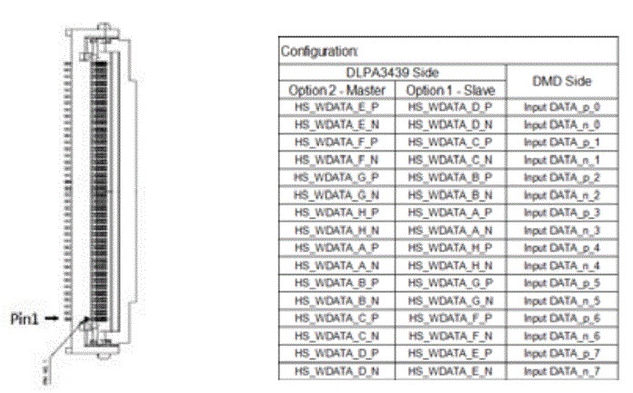
    in the schematic file of dlp4710 (tidrnb9.pdf) we see a connection table in page 7 (why dlpa3439 instead of dlpc3439 ???)

    but in dlpc3439 datasheet in page 39 we see another connection table


    why these two above table are not equal?

    for example for "Input DATA_p_0" :

    in "tidrnb9.pdf" => Master=HS_WDATA_E_P   Slave=HS_WDATA_D_P

    in "dlpc3439.pdf" => Master=HS_WDATA_D_P   Slave=HS_WDATA_E_P


    which one of them are true?


    What is the "swap control"?

    Best Regards


  • Jack,

    The table cell reading "DLPA3439" is an error. It should instead read "DLPC3439".

    The swap control refers to the pin mapping order (which is software configurable between two different potential settings) from the controller to the DMD. I recommend referring to the DMD pin mapping swap control table in the DLPC3439 datasheet, as it is less confusing in this case. They are both technically correct though.

    Regards,

    Philippe Dollo

  • Hi Phillippe,

    Pls more explain for me.

    I did not find any software control for pin mapping order in any pdf files about dlpc3439! Only a pin for master and slave selection.

    And in page 39 of dlpc3439 datasheet in 8.3.10 dmd(sub-lvds) interface I see a table that is not same as the table in "tidrnb9.pdf" page 7?

    Master and slave configuration is vice versa in two table!!!

    And I can not find "swap control" in any pdf files about dlpc3439! 

    Best Regards

  • Jack,

    Our team is looking into your queries and will get back to you soon. 

    Your patience is appreciated.

    Regards,

    Mayank

  • Hi Mayank,

    What's up?

    I'm waiting for you

    Best Regards

  • Jack,

    The "Swap Control" you are referring to is actually built into the firmware itself. That is to say, the firmware binary that you load to your system is pre-configured to work with a specific "Swap Control" setting, which is also referred to as "Pin Mapping Option".

    We have a firmware selector tool available which allows users to download the alternative configurations, if they are designing their own board and cannot make use of the default EVM firmware. In the case of this EVM, the DLPC3439 is the controller used, and two pin mapping options are available (1 and 2, which is equivalent to Swap Control settings 0 and 1).

    The firmware selector tool can be accessed at [ http://software-dl.ti.com/dlp/pico-fw-selector/ ]

    I hope this helps.

    Regards,
    Philippe Dollo

  • Hi Philippe,

    Thanks for your answer.

    But that was not the answer to all my questions! I was asked:

    "And in page 39 of dlpc3439 datasheet in 8.3.10 dmd(sub-lvds) interface I see a table that is not same as the table in "tidrnb9.pdf" page 7?

    Master and slave configuration is vice versa in two table!!!"

    I know this chip has two pin mapping option but I see two tables in the schematic files and datasheet of this chip that are opposite to each other !!! why?

    I was check the board of eval module and datasheet seems to be wrong!

    in page 7 of schematic, I see:

    in page 39 of datasheet, I see:

    for example for "Input DATA_p_0" :

    in "tidrnb9.pdf" => Master=HS_WDATA_E_P   Slave=HS_WDATA_D_P

    in "dlpc3439.pdf" => Master=HS_WDATA_D_P   Slave=HS_WDATA_E_P

    Best Regards

  • Hi Jack,

    Thank you for bringing this to our attention. We will look into this and get back to you shortly.

    Regards,

    Austin

  • Hello Jack,

    Thank you. There is mistake in the datasheet. We will update the datasheet to include other pin mapping information in future. Meanwhile , you may use DLPC3479 datasheet for the pin mapping. This controller has similar functionality and datasheet is updated.

    regards,

    Vivek