This thread has been locked.

If you have a related question, please click the "Ask a related question" button in the top right corner. The newly created question will be automatically linked to this question.

TMS320C5505: ISSI 1MegBits x 16Bits x 4Banks (64-MBIT) SDRAM issue - last 320K inaccessible / memory tests fail

Part Number: TMS320C5505

Hi,

I'm having trouble with an ISSI 1MegBits x 16Bits x 4Banks (64-MBIT) SDRAM. It's organized as 4 banks of 4,096 rows by 256 columns by 16 bits, for a total of 4Meg Words (16-bit bytes for the DSP). It's being used in a custom DSP system with a 16-bit data bus and a 12-bit address bus with 2 lines for bank access of 4 banks.

The configuration and initialization seems to be correctly done, as I do the memory tests the data bus checks out OK. However the address bus tests fail and the device integrity tests fails, and these last two tests fail at the same address which turns out to be the memory address 0x3B 0000 (with the start being at 0x0 0000).

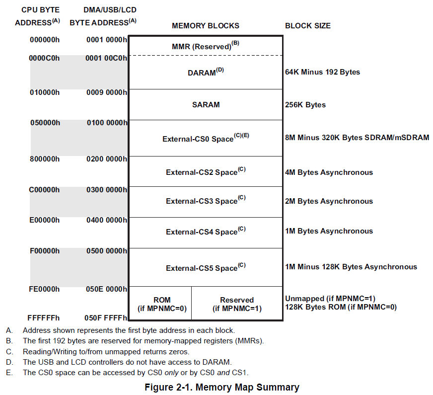
The actual DSP external memory mapping is from 0x5 0000 to 0x45 0000, but above I've subtracted the offset for simplicity. This mapping is taken from page 16 of the sprugu6b, TMS320C55xx External Memory Interface (EMIF) Users Guide.

So the DSP should be able to address beyond the 0x40 0000 DSP memory address all the way from 0x5 0000 to 0x45 0000, but it seems to fail and get stuck consistently beyond this 0x40 0000 address.

If I redefine the external memory map to be only from 0x5 0000 to 0x40 0000, and limit the tests to this memory region then obviously ALL 3 tests pass consitently. So there's the remaining 0x5 0000 (327680 or 320K) memory bytes (words) that cannot be accessed and I can't work out why this may be the case ? It's just a coincidence that this remaining 320K Words is a problem, not only on the first custom board prototype but on the second revision also ! It would appear the electrical interfacing is correct and the EMIF configuration also. Sure we could probably leave out the last 320K Words of external memory as we will never use the full 4Meg Words of external SDRAM, but it may just be something very simple that I've overlooked in the initialization or something else to do with the EMIF ?!?

BTW the SDRAM and the DSP both come in BGA packages with dense multilayer routing so access to the control lines is limited for probing without some fine soldering ... the Bank select pins are routed on the top layer so I can access these more easily ...

So my question is what could cause the memory test errors beyond the 0x40 000 memory address, which makes the SDRAM access short of 320K bytes (here a byte is 16-bits).

Thanks in advance,

Mike

  • Hi Mike,

    The SDRAM memory map should span from byte addresses...
    0x50000 to 0x800000, but you are only getting...
    0x50000 to 0x400000, correct?

    I'm not immediately sure what could be going on. Can you figure out the physical address that is used beyond 0x400000?

    Does writing beyond 0x400000 corrupt any lower memory addresses?

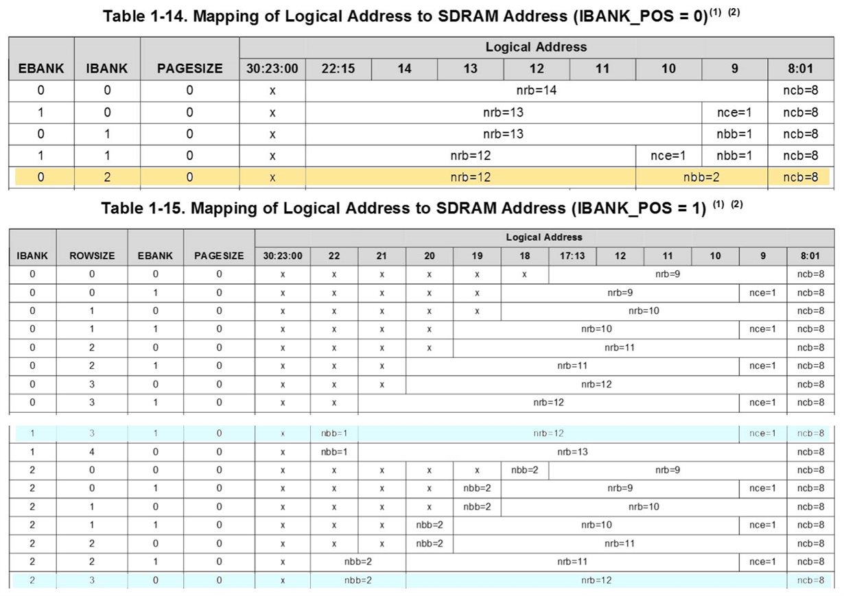
    What settings are you Mapping from Logical Address to SDRAM Address?

    Refer to SPRUGU6B 1.2.6.11 Mapping from Logical Address to SDRAM Address
    Table 1-14. Mapping of Logical Address to SDRAM Address (IBANK_POS = 0)(1) (2)
    Table 1-15. Mapping of Logical Address to SDRAM Address (IBANK_POS = 1) (1) (2)

    Regards,
    Mark

  • Mark Mckeown said:

    Hi Mike,

    The SDRAM memory map should span from byte addresses...
    0x50000 to 0x800000, but you are only getting...
    0x50000 to 0x400000, correct?

    I'm not immediately sure what could be going on. Can you figure out the physical address that is used beyond 0x400000?

    Does writing beyond 0x400000 corrupt any lower memory addresses?

    What settings are you Mapping from Logical Address to SDRAM Address?

    Hi Mark,

    Yes, as I was saying the memory is organized as 12 rows bits x 8 columns bits x 2 bank bits x 16-bits which amounts to 64Mbit, or 0x40 0000 16-bit bytes capacity.

    So according to the map you show above the CS0 external space starts at 0x5 0000 and should end at 0x45 0000.

    The tests start failing at address 0x40 0000 which leaves me 320K short of what I was expecting. This is too much of a coincidence as the map shown above shows the CS0 accessibe amount is 8Mbits - 320Kbits. But I don't have a full 8Mbit SDRAM, so I was expecting to go to 0x 45 0000 without an issue.

    So in the document SPRUGU6B the tables below sumerize the mappings of logical addresses :

    My current setting is highlighted in orange. The SDRAM has 12 address bits of which 12 rows and 8 column bits multiplexed, 2 bits for the 4 banks, and 1 Chip Select. In the table above I don't see any cases with nce>1 so I assume when more than one CS is used then nce=1. I have ncb=8, nrb=12 and nbb=2 so the best options above are highlighted. In my case I only have one CS for chip access and the only other better configuration setting could be the second blue highlited one in Table 1-15. I haven't tried it yet, but which one would you recommend in your opinion and why should the orange one be giving me issues ?

    Another question relates to the CS0 memory space in the table you show. It says the space is accessible only by CS0, or by CS0 and CS1. I hav't checked yet but where is this setting chosen ? I assume if both CS0 and CS1 are used for the CS0 space then there will be a boundry break in the space somewhere, and this boundry could be where I'm  starting to see a requirement for CS1 access which I don't have as its not wired up - only CS0 is wired to the SDRAM.

    Any thoughts on this, suggestions ?

    Best Regards,

    Mike

  • citizen said:

    Another question relates to the CS0 memory space in the table you show. It says the space is accessible only by CS0, or by CS0 and CS1. I hav't checked yet but where is this setting chosen ? I assume if both CS0 and CS1 are used for the CS0 space then there will be a boundry break in the space somewhere, and this boundry could be where I'm  starting to see a requirement for CS1 access which I don't have as its not wired up - only CS0 is wired to the SDRAM.

    Any thoughts on this, suggestions ?

    Best Regards,

    Mike

    Hi Mark,

    I think the IBANK_POS = 0 setting above should be OK, and this shows to be OK with CS0 use, and going from 0x5 0000 to 0x40 0000.

    So my question still stands for clarification. If I use 2 chips of 1MegBits x 16Bits x 4Banks and both CS0 and CS1 on each of the devices respectively, then I should be able to access "8M - 320K" in the CS0 external space. This implies that one of the chips will have 320K less accessible memory than expected. So this is not documented in the application note ... which of the devices would have less accessible memory, the CS0 device or the CS1 device ? If I were to use a 2MegBits x 16Bits x 4Banks with CS0 then this would be 8M - 320K of accessible memory in total, as indicated in the memory map, so this would be as expected I guess ... What I wasn't expecting is that with half the memory used in the CS0 memory space, I am accessing only 4M - 320K instead of the full 4Meg.

    Cheers, Mike

  • Hi Mike,

    Sorry for dropping the ball here..

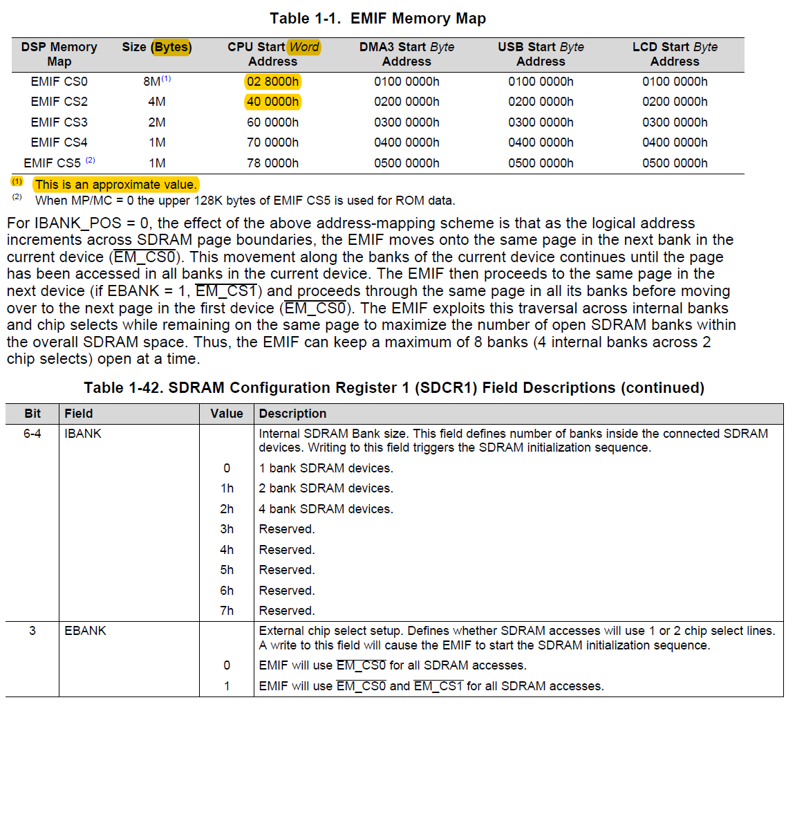
    Maybe this table from the EMIF User's guide is better.

    The C55xx is a 16-bit machine, so all accesses will be 16-bit words (not bytes). You can multiply by two to get the bytes, but all accesses are 16-bit.

    the EMIF CS0 range (including CS1) can be calculated as 0x400000 - 0x28000 = 3.84375MegaWords (not 4 MegaWords). 

    EBANK decides whether one CS0 or two CS0/CS1 will be used.

    Regards,
    Mark

  • Hi Mark,

    This is ok for me. the EBANK value is 0 and the IBANK is 2 (4 banks). There is 320K inaccessible as suggested and that's OK, we can afford that.

    Regards,

    Mike