This thread has been locked.

If you have a related question, please click the "Ask a related question" button in the top right corner. The newly created question will be automatically linked to this question.

TUSB8020B-Q1: TUSB8020 cannot be detected through the i2c bus

Part Number: TUSB8020B-Q1
Other Parts Discussed in Thread: TUSB8020B

Hi Team,

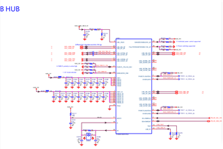
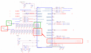
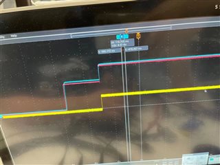
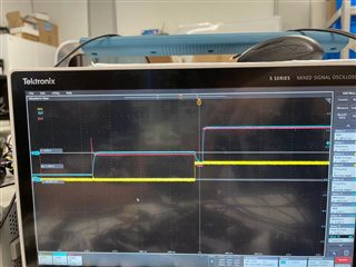
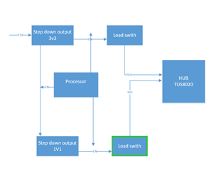
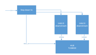
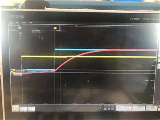
After measuring each power pin, the voltage is normal and meets the power-on sequence in the datasheet. But now the usb port is still unusable, and the usb8020 chip cannot be detected through the i2c bus, so it is suspected that the chip is not working properly. 

Could you kindly give some help?

  • Hi Amelie,

    Schematic feedback:

    • There is an internal pullup on the GRSTz pin, we do not recommend the external pullup be installed on this pin.
    • Installing a pullup on a PWRCTLx output will enable battery charging mode on that port if the hub is configured through pin configurations.

    If SMBUSz is high and no EEPROM is attached, does the hub connect?  If not, can you check that USB_VBUS pin voltage is around 500 mV?  Also, what are the line states on DP and DM of the upstream facing USB 2.0 port?

    If the hub is configured for I2C mode, it will operate in I2C master mode and after the power on reset, it will look for an attached EEPROM.  If it does not see an EEPROM, it will load in the pin configurations and function as a hub.

    If the hub is configured for SMBUS mode, it will operate in SMBUS slave mode and after the power on reset, it will wait to be configured by a SMBUS master.  It will not connect as a hub until the SMBUS host sets the cfgactive bit in the registers.

    What address is your SMBUS/I2C master checking for?  It sounds like your application is a SMBUS application, not an I2C one.  Most I2C hosts can be used with the SMBUS mode of the TUSB8020B.

    Regards,

    JMMN

  • Hi, JMMN

    1. We have found current leakage on pin VDD_3V3(7,13,23...pins on TUS8020),which lead to a 0.9V voltage drop on these pins before we provided an 3.3V power supply.  We have checked all of the peripheral circuit of the TUS8020, and we finnally found that it was the SMbus line which lead  to the leakage on the VDD 3V3 pins , while the VDD 1V1 pins seems operates all right ,  so could you help us with this confusing issue ,and may i have the internal block diagram of TUS8020 so that we can find out the relationship between SMbus line and the VDD 3V3 pins?

    2.We tested the power on sequence and found VDD_1v1 is  before VDD_3v3 1ms (RST signal timing is correct), at this time, both hot and cold start have problems, as shown in Figure 2-1; Software controlled VDD_1v1 after VDD_3v3, RST signal is normal, and the cold and hot start is ok, but the power on sequence is very chaotic, as shown in Figure 2-2. Please confirm the power on VDD_ 1v1 early than VDD_3v3 1ms whether has problem,  and please help to analyze the waveform of our software after power on according to the normal time sequence.

    3.USB1 VBUS in downstream does not work normally when it is not connected with power supply

  • Hi Dai Xinyu,

    1. Can you confirm that the hub is left powered off, but connected to powered SDA / SCL lines?   The hub has internal pulldowns on the SDA/SCL pins that are likely drawing power in this case, but since the hub is only partially powered, device operation is undefined.  Since SMBUS mode is not enabled, I would recommend disconnecting these pins.

    2.  Neither of the scope plots look normal.  The 1.1V rail looks ok, but the 3.3V rail being held in a partially powered state will cause unexpected behaviors.  Why is the 3.3V level being held low?  What kind of regulator is providing power? The reset will only work if the power rails are at the expected levels when it occurs.

    3.  Can you explain this in more detail?  Battery charging is enabled on both downstream ports, so the power switches will be enabled when there is no host controller present and then re-enabled when a host controller is attached.  Can you share the power switch design?  Where are the downstream power switches sourced from?

    Regards,

    JMMN

  • Hi, JMMN

    1. The picture is captured when vdd_1v1 nad vdd_3v3 is normal enable. We found electric leakage (IIC)when we disable vdd_1v1 and vdd_3v3. There is no input at power source of downstream. So we think leakage is the cause of IIC. What is the pull-down resistance? Why IIC leakage would affect vdd_3v3?

    2. Our Soc enable vdd_1v1 and vdd_3v3 when system power up. There is no other operatiion with hub chip. We think vdd_3v3 not pull up 3.3v right away is cause of the unknown circuit in hub chip. The power control picture is shown as below. And we also want to know can we use uncontrollable fixed power supply for peripheral configuration such as SMBUSZ/SS_DN2/GRSTZ/PWRCTL_POL/SS_DN1/OVERCUR1Z?

    3.The power switch design is shown as below.


  • Hi Dai Xinyu,

    1. The I2C cells are powered from 3.3V so this is why the leakage shows up there.  The pulldowns are typically 150 uA or approximately 22 Kohm.

    2.  Since the application is not using SMBUS, I would recommend disconnecting it from the I2C bus to prevent the leakage.  The other IO can be set by regular pullup / pulldowns.

    Regards,

    JMMN

  • Hi JMMN

    Please check the power sequence. We disconnect the IIC.

  • Yes, that looks correct.  Is the customer able to see reliable performance on reset / boot?

    The 1.1V rail can ramp closer to 3.3V if needed, but current implementation looks acceptable.

    Regards,

    JMMN