This thread has been locked.

If you have a related question, please click the "Ask a related question" button in the top right corner. The newly created question will be automatically linked to this question.

PCA9306-Q1: Please review the schematic

Part Number: PCA9306-Q1

Hello TI experts,

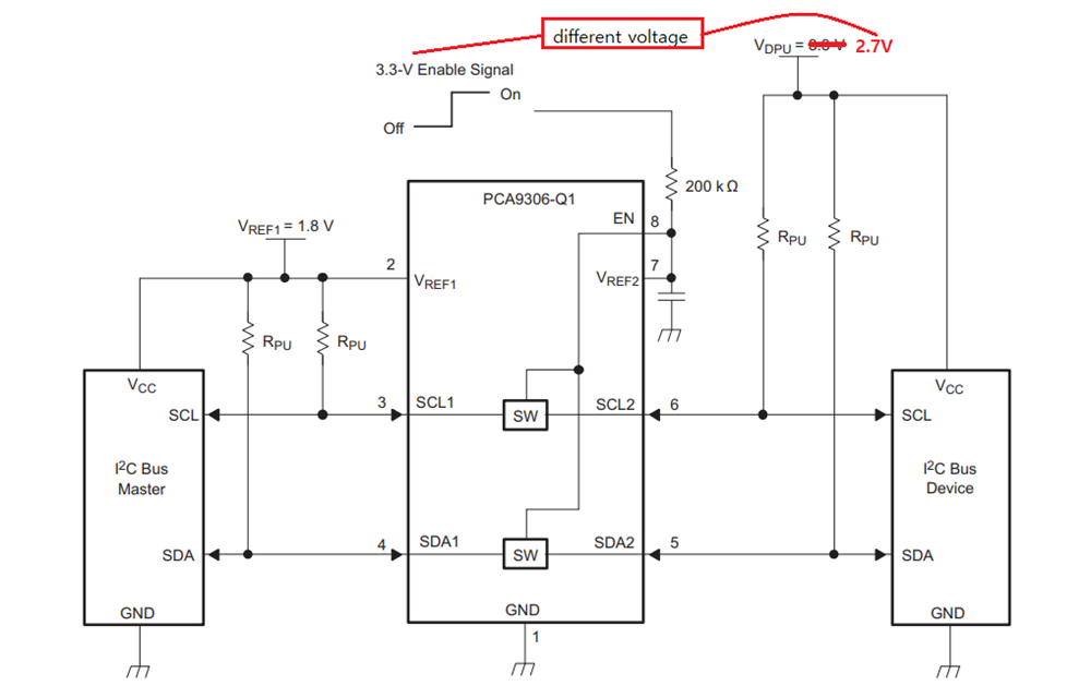
My customer drew their first schematic with PCA9306-Q1. Could you review the schematic?

and here are some question.

1. they wanted to separate EN and VREF2. is it possible?

they want that VREF1 and VREF2 is already powered, and only EN pin would change.

I also saw that I have to remain Hi-Z state instead of low, if I want to disable IC. (active high is fine) is it right?

2. if separation is possible, do we need to use 200kohm each of the line?

3. is there any limitation about the voltage of EN pin?

and please tell me if there are any suggestions for this schematic.

Best regards,

Chase

  • EN and VREF2 must be connected together. The resistor is needed to limit the current flowing into VREF2.

    If you want to control EN externally, you have to drive it from an open-drain output (actively driven low, Hi-Z instead of high).

    See [FAQ] How do the LSF translators work?

  • Hi Chase,

    As Clemens said, the EN and VREF2 pins must be shorted together for this device to work in translation mode:

    There are limitations on the EN pin voltage. First, no pin can be driven higher than 7V. The recommended EN input voltage is from 0 - 5.5V.

    You can actually control the EN pin by using a switch on the VCC2 voltage:

    Here VREF2 and EN are still shorted together but the input voltage is now controlled with a switch. As you can see the voltage going into VREF2 does not have to be the same voltage you pull the SDA and SCL lines up to. So you can control both of those pins using a GPIO pin.

    The rest of the schematic looks good. I also recommend checking the pull up resistors using this document.

    Best,

    Chris

  • Hi Clemens, Chris,

    Thank you for your reply.

    I understand that EN and VREF must be tied together.

    what I want to know is, it is okay that the voltage of VREF2 and pull up voltage(V_dpu) is different.

    based on you said(Chris), i can design the schematic as below.

    Please check this schematic (especially the voltage difference between VREF2 and V-dpu) is right.

    Best regards,

    Chase

  • This is OK; all pull-up voltages can be different. The only restrictions are the minimal voltage difference between VREF1 and VREF2, and that VREF1 must not be larger than any signal voltage.

  • Hi Clemens,

    Thank you for your reply.

    I have more questions.

    1. how about the value of filter capacitor of VREF2? is 100pF okay? (same as normal schematic)

    2. you said that EN input should be open drain output from MCU or something (0 and Hi-Z) what would be happen if I apply 1(high=3.3V) on EN pin?

    please check these issues. Thanks.

    Best regards,

    Chase

  • 1. The capacitor is not required, so any value is OK. But it is charged through the 200k resistor, so it should not be too large if you do not want EN to rise very slowly.

    2. When you force EN to 3.3 V, signals on the left side will be clamped at a voltage larger than 1.8 V.