This thread has been locked.

If you have a related question, please click the "Ask a related question" button in the top right corner. The newly created question will be automatically linked to this question.

TCAN1042HGV-Q1: Leakage path and internal diode structures

Part Number: TCAN1042HGV-Q1

Hi TI team,

We are currently working on a project that has a really tight sleep current requirement and we request your help in finding out leakage current from TCAN IC. During the sleep mode of our device, only the 3.3V supply will be present and the 5V supply will be inactive. STB will be set high during sleep mode.

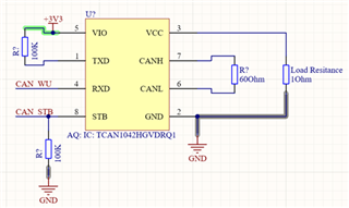
On the datasheet of TCAN1042, we find that the standby supply current is 17uA max. But we would like to know the entire current (supply + leakage currents) of TCAN when only the VIO supply is present and VCC is loaded as shown in the snippet below

CAN_loaded_sleep

If possible can you share the internal body structure of TCAN1042 IC? It would help us a lot in the assessment of sleep currents on the CAN section of our board.


  • Hi Ashwath,

    There is no leakage path between Vio and Vcc, so not current will leak from the enabled Vio supply to the loaded Vcc pin in this configuration. 

    The calculations for this can be simplified by only looking at the supply to Vio and the leakage through the digital input pins TXD and STB. The Vio as you stated will use a maximum of 17uA in sleep mode. The two input pins will combined sink a maximum of 3uA while driven to Vio levels based on the datasheet, though real leakage through these pins in a normal setup will be less as they are internally biased to Vio. 

    Let me know if this is sufficient for your low-power consumption calculations and if you have any more questions. 

    Regards,
    Eric Schott