This thread has been locked.

If you have a related question, please click the "Ask a related question" button in the top right corner. The newly created question will be automatically linked to this question.

DS90UB940-Q1EVM: dimensions

Part Number: DS90UB940-Q1EVM
Other Parts Discussed in Thread: DS90UB940-Q1

Hi TI support team,

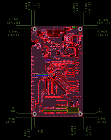
could you provide a technical drawing of the eval board DS90UB940-Q1 EVM please? I have to mount this board into a housing where I have to drill holes for the connectors. Furthermore I want to contact the CSI-2 connectors with a PCB.

best regards
Peter

  • Hi Peter,

    Let me look at the design file, and I will get back with you by Monday, 7/19.

    Aaron

  • Hi Aaron,

    that sounds good. Thank you very much

    Peter

  • Hi Peter,

    No worries. I will get the dimension soon.

    Aaron

  • Hi Aaron, thanks a lot.
    In addition to the board dimensions I will need the drilling and connector positions, especially J13, J15 and J16

    Peter

  • Hi Peter,

    Thank you so much for your patience. I was able to find the design file. Below is the information that you are looking for.

    This is the board dimension for 940EVM as well as the dimension for four mounting holes.

    Here is the J15 and 16 drill holes information and the position of the connector at pin 1.

    Here is J13 information.

    Attached are the files for patstack information.

    J13 Connector

    J13_S63H43.html
    <h2><b><center>S63H43</b></center></h2>
    <body>
    <large>
    <br>date/time: 2021/07/19 10:34:03<br>
    <br>type: Through Pin
    <br>units: mils
    <br>decimal places: 2
    <br><br><u>Hole data</u><blockquote>
    geometry: Circle
    <br>size: 40.00
    <br>offset: (0.00, 0.00)
    <br>tolerance: positive=2.00 negative=2.00
    <br>plating: Plated
    </blockquote>
    <br><u>Drill symbol data</u><blockquote>
    geometry: Circle
    <br>width: 43.00
    <br>height: 43.00
    <br>characters: M
    </blockquote>
    <br><u>Design layer pads</u>
    <blockquote>Layer: TOP
    <table border=1>
    <tr>
    <th>Pad</th>
    <th>Geometry</th>
    <th>Width</th>
    <th>Height</th>
    <th>X offset</th>
    <th>Y offset</th>
    </tr>
    <tr>
    <td>Regular</td>
    <td>Square</td>
    <td>63.00</td>
    <td>63.00</td>
    <td>0.00</td>
    <td>0.00</td>
    </tr>
    <tr>
    <td>Thermal</td>
    <td>Square</td>
    <td>83.00</td>
    <td>83.00</td>
    <td>0.00</td>
    <td>0.00</td>
    </tr>
    <tr>
    <td>Anti</td>
    <td>Square</td>
    <td>83.00</td>
    <td>83.00</td>
    <td>0.00</td>
    <td>0.00</td>
    </tr>
    <tr>
    <td>Keep Out</td>
    <td>None</td>
    </tr>
    </table><br>
    </blockquote>
    <blockquote>Layer: GND
    <table border=1>
    <tr>
    <th>Pad</th>
    <th>Geometry</th>
    <th>Width</th>
    <th>Height</th>
    <th>X offset</th>
    <th>Y offset</th>
    </tr>
    <tr>
    <td>Regular</td>
    <td>Round</td>
    <td>63.00</td>
    <td>63.00</td>
    <td>0.00</td>
    <td>0.00</td>
    </tr>
    <tr>
    <td>Thermal</td>
    <td>Round</td>
    <td>83.00</td>
    <td>83.00</td>
    <td>0.00</td>
    <td>0.00</td>
    </tr>
    <tr>
    <td>Anti</td>
    <td>Round</td>
    <td>83.00</td>
    <td>83.00</td>
    <td>0.00</td>
    <td>0.00</td>
    </tr>
    <tr>
    <td>Keep Out</td>
    <td>None</td>
    </tr>
    </table><br>
    </blockquote>
    <blockquote>Layer: POWER
    <table border=1>
    <tr>
    <th>Pad</th>
    <th>Geometry</th>
    <th>Width</th>
    <th>Height</th>
    <th>X offset</th>
    <th>Y offset</th>
    </tr>
    <tr>
    <td>Regular</td>
    <td>Round</td>
    <td>63.00</td>
    <td>63.00</td>
    <td>0.00</td>
    <td>0.00</td>
    </tr>
    <tr>
    <td>Thermal</td>
    <td>Round</td>
    <td>83.00</td>
    <td>83.00</td>
    <td>0.00</td>
    <td>0.00</td>
    </tr>
    <tr>
    <td>Anti</td>
    <td>Round</td>
    <td>83.00</td>
    <td>83.00</td>
    <td>0.00</td>
    <td>0.00</td>
    </tr>
    <tr>
    <td>Keep Out</td>
    <td>None</td>
    </tr>
    </table><br>
    </blockquote>
    <blockquote>Layer: DEFAULT INTERNAL
    <table border=1>
    <tr>
    <th>Pad</th>
    <th>Geometry</th>
    <th>Width</th>
    <th>Height</th>
    <th>X offset</th>
    <th>Y offset</th>
    </tr>
    <tr>
    <td>Regular</td>
    <td>Round</td>
    <td>63.00</td>
    <td>63.00</td>
    <td>0.00</td>
    <td>0.00</td>
    </tr>
    <tr>
    <td>Thermal</td>
    <td>Round</td>
    <td>83.00</td>
    <td>83.00</td>
    <td>0.00</td>
    <td>0.00</td>
    </tr>
    <tr>
    <td>Anti</td>
    <td>Round</td>
    <td>83.00</td>
    <td>83.00</td>
    <td>0.00</td>
    <td>0.00</td>
    </tr>
    <tr>
    <td>Keep Out</td>
    <td>None</td>
    </tr>
    </table><br>
    </blockquote>
    <blockquote>Layer: BOTTOM
    <table border=1>
    <tr>
    <th>Pad</th>
    <th>Geometry</th>
    <th>Width</th>
    <th>Height</th>
    <th>X offset</th>
    <th>Y offset</th>
    </tr>
    <tr>
    <td>Regular</td>
    <td>Square</td>
    <td>63.00</td>
    <td>63.00</td>
    <td>0.00</td>
    <td>0.00</td>
    </tr>
    <tr>
    <td>Thermal</td>
    <td>Square</td>
    <td>83.00</td>
    <td>83.00</td>
    <td>0.00</td>
    <td>0.00</td>
    </tr>
    <tr>
    <td>Anti</td>
    <td>Square</td>
    <td>83.00</td>
    <td>83.00</td>
    <td>0.00</td>
    <td>0.00</td>
    </tr>
    <tr>
    <td>Keep Out</td>
    <td>None</td>
    </tr>
    </table><br>
    </blockquote>
    <blockquote>Layer: ADJACENT LAYER
    <table border=1>
    <tr>
    <th>Pad</th>
    <th>Geometry</th>
    <th>Width</th>
    <th>Height</th>
    <th>X offset</th>
    <th>Y offset</th>
    </tr>
    <tr>
    <td>Regular</td>
    <td>None</td>
    </tr>
    <tr>
    <td>Thermal</td>
    <td>None</td>
    </tr>
    <tr>
    <td>Anti</td>
    <td>None</td>
    </tr>
    <tr>
    <td>Keep Out</td>
    <td>None</td>
    </tr>
    </table><br>
    </blockquote>
    <br><u>Mask layer pads</u>
    <blockquote>
    <table border=1>
    <tr>
    <th>Layer</th>
    <th>Geometry</th>
    <th>Width</th>
    <th>Height</th>
    <th>X offset</th>
    <th>Y offset</th>
    </tr>
    <tr>
    <td>SOLDERMASK_TOP</td>
    <td>Square</td>
    <td>66.00</td>
    <td>66.00</td>
    <td>0.00</td>
    <td>0.00</td>
    </tr>
    <tr>
    <td>SOLDERMASK_BOTTOM</td>
    <td>Square</td>
    <td>66.00</td>
    <td>66.00</td>
    <td>0.00</td>
    <td>0.00</td>
    </tr>
    <tr>
    <td>PASTEMASK_TOP</td>
    <td>None</td>
    </tr>
    <tr>
    <td>PASTEMASK_BOTTOM</td>
    <td>None</td>
    </tr>
    <tr>
    <td>FILMMASK_TOP</td>
    <td>None</td>
    </tr>
    <tr>
    <td>FILMMASK_BOTTOM</td>
    <td>None</td>
    </tr>
    <tr>
    <td>COVERLAY_TOP</td>
    <td>None</td>
    </tr>
    <tr>
    <td>COVERLAY_BOTTOM</td>
    <td>None</td>
    </tr>
    </table><br>
    </blockquote>
    <br><u>Usage options</u><blockquote>
    Suppress unconnected internal pads: Yes
    <br>Lock layer span: No
    </body>
    

    J13_C63H43.html
    <h2><b><center>C63H43</b></center></h2>
    <body>
    <large>
    <br>date/time: 2021/07/19 10:35:16<br>
    <br>type: Through Pin
    <br>units: mils
    <br>decimal places: 2
    <br><br><u>Hole data</u><blockquote>
    geometry: Circle
    <br>size: 40.00
    <br>offset: (0.00, 0.00)
    <br>tolerance: positive=2.00 negative=2.00
    <br>plating: Plated
    </blockquote>
    <br><u>Drill symbol data</u><blockquote>
    geometry: Circle
    <br>width: 43.00
    <br>height: 43.00
    <br>characters: M
    </blockquote>
    <br><u>Design layer pads</u>
    <blockquote>Layer: TOP
    <table border=1>
    <tr>
    <th>Pad</th>
    <th>Geometry</th>
    <th>Width</th>
    <th>Height</th>
    <th>X offset</th>
    <th>Y offset</th>
    </tr>
    <tr>
    <td>Regular</td>
    <td>Round</td>
    <td>63.00</td>
    <td>63.00</td>
    <td>0.00</td>
    <td>0.00</td>
    </tr>
    <tr>
    <td>Thermal</td>
    <td>Round</td>
    <td>83.00</td>
    <td>83.00</td>
    <td>0.00</td>
    <td>0.00</td>
    </tr>
    <tr>
    <td>Anti</td>
    <td>Round</td>
    <td>83.00</td>
    <td>83.00</td>
    <td>0.00</td>
    <td>0.00</td>
    </tr>
    <tr>
    <td>Keep Out</td>
    <td>None</td>
    </tr>
    </table><br>
    </blockquote>
    <blockquote>Layer: GND
    <table border=1>
    <tr>
    <th>Pad</th>
    <th>Geometry</th>
    <th>Width</th>
    <th>Height</th>
    <th>X offset</th>
    <th>Y offset</th>
    </tr>
    <tr>
    <td>Regular</td>
    <td>Round</td>
    <td>63.00</td>
    <td>63.00</td>
    <td>0.00</td>
    <td>0.00</td>
    </tr>
    <tr>
    <td>Thermal</td>
    <td>Round</td>
    <td>83.00</td>
    <td>83.00</td>
    <td>0.00</td>
    <td>0.00</td>
    </tr>
    <tr>
    <td>Anti</td>
    <td>Round</td>
    <td>83.00</td>
    <td>83.00</td>
    <td>0.00</td>
    <td>0.00</td>
    </tr>
    <tr>
    <td>Keep Out</td>
    <td>None</td>
    </tr>
    </table><br>
    </blockquote>
    <blockquote>Layer: POWER
    <table border=1>
    <tr>
    <th>Pad</th>
    <th>Geometry</th>
    <th>Width</th>
    <th>Height</th>
    <th>X offset</th>
    <th>Y offset</th>
    </tr>
    <tr>
    <td>Regular</td>
    <td>Round</td>
    <td>63.00</td>
    <td>63.00</td>
    <td>0.00</td>
    <td>0.00</td>
    </tr>
    <tr>
    <td>Thermal</td>
    <td>Round</td>
    <td>83.00</td>
    <td>83.00</td>
    <td>0.00</td>
    <td>0.00</td>
    </tr>
    <tr>
    <td>Anti</td>
    <td>Round</td>
    <td>83.00</td>
    <td>83.00</td>
    <td>0.00</td>
    <td>0.00</td>
    </tr>
    <tr>
    <td>Keep Out</td>
    <td>None</td>
    </tr>
    </table><br>
    </blockquote>
    <blockquote>Layer: DEFAULT INTERNAL
    <table border=1>
    <tr>
    <th>Pad</th>
    <th>Geometry</th>
    <th>Width</th>
    <th>Height</th>
    <th>X offset</th>
    <th>Y offset</th>
    </tr>
    <tr>
    <td>Regular</td>
    <td>Round</td>
    <td>63.00</td>
    <td>63.00</td>
    <td>0.00</td>
    <td>0.00</td>
    </tr>
    <tr>
    <td>Thermal</td>
    <td>Round</td>
    <td>83.00</td>
    <td>83.00</td>
    <td>0.00</td>
    <td>0.00</td>
    </tr>
    <tr>
    <td>Anti</td>
    <td>Round</td>
    <td>83.00</td>
    <td>83.00</td>
    <td>0.00</td>
    <td>0.00</td>
    </tr>
    <tr>
    <td>Keep Out</td>
    <td>None</td>
    </tr>
    </table><br>
    </blockquote>
    <blockquote>Layer: BOTTOM
    <table border=1>
    <tr>
    <th>Pad</th>
    <th>Geometry</th>
    <th>Width</th>
    <th>Height</th>
    <th>X offset</th>
    <th>Y offset</th>
    </tr>
    <tr>
    <td>Regular</td>
    <td>Round</td>
    <td>63.00</td>
    <td>63.00</td>
    <td>0.00</td>
    <td>0.00</td>
    </tr>
    <tr>
    <td>Thermal</td>
    <td>Round</td>
    <td>83.00</td>
    <td>83.00</td>
    <td>0.00</td>
    <td>0.00</td>
    </tr>
    <tr>
    <td>Anti</td>
    <td>Round</td>
    <td>83.00</td>
    <td>83.00</td>
    <td>0.00</td>
    <td>0.00</td>
    </tr>
    <tr>
    <td>Keep Out</td>
    <td>None</td>
    </tr>
    </table><br>
    </blockquote>
    <blockquote>Layer: ADJACENT LAYER
    <table border=1>
    <tr>
    <th>Pad</th>
    <th>Geometry</th>
    <th>Width</th>
    <th>Height</th>
    <th>X offset</th>
    <th>Y offset</th>
    </tr>
    <tr>
    <td>Regular</td>
    <td>None</td>
    </tr>
    <tr>
    <td>Thermal</td>
    <td>None</td>
    </tr>
    <tr>
    <td>Anti</td>
    <td>None</td>
    </tr>
    <tr>
    <td>Keep Out</td>
    <td>None</td>
    </tr>
    </table><br>
    </blockquote>
    <br><u>Mask layer pads</u>
    <blockquote>
    <table border=1>
    <tr>
    <th>Layer</th>
    <th>Geometry</th>
    <th>Width</th>
    <th>Height</th>
    <th>X offset</th>
    <th>Y offset</th>
    </tr>
    <tr>
    <td>SOLDERMASK_TOP</td>
    <td>Round</td>
    <td>66.00</td>
    <td>66.00</td>
    <td>0.00</td>
    <td>0.00</td>
    </tr>
    <tr>
    <td>SOLDERMASK_BOTTOM</td>
    <td>Round</td>
    <td>66.00</td>
    <td>66.00</td>
    <td>0.00</td>
    <td>0.00</td>
    </tr>
    <tr>
    <td>PASTEMASK_TOP</td>
    <td>None</td>
    </tr>
    <tr>
    <td>PASTEMASK_BOTTOM</td>
    <td>None</td>
    </tr>
    <tr>
    <td>FILMMASK_TOP</td>
    <td>None</td>
    </tr>
    <tr>
    <td>FILMMASK_BOTTOM</td>
    <td>None</td>
    </tr>
    <tr>
    <td>COVERLAY_TOP</td>
    <td>None</td>
    </tr>
    <tr>
    <td>COVERLAY_BOTTOM</td>
    <td>None</td>
    </tr>
    </table><br>
    </blockquote>
    <br><u>Usage options</u><blockquote>
    Suppress unconnected internal pads: Yes
    <br>Lock layer span: No
    </body>
    

    J15 and J16 Connectors

    J15_J16_S35H63.html
    <h2><b><center>S35H63</b></center></h2>
    <body>
    <large>
    <br>date/time: 2021/07/19 10:31:29<br>
    <br>type: Through Pin
    <br>units: mils
    <br>decimal places: 2
    <br><br><u>Hole data</u><blockquote>
    geometry: Circle
    <br>size: 40.00
    <br>offset: (0.00, 0.00)
    <br>tolerance: positive=3.00 negative=3.00
    <br>plating: Plated
    </blockquote>
    <br><u>Drill symbol data</u><blockquote>
    geometry: Circle
    <br>width: 40.00
    <br>height: 40.00
    <br>characters: S
    </blockquote>
    <br><u>Design layer pads</u>
    <blockquote>Layer: TOP
    <table border=1>
    <tr>
    <th>Pad</th>
    <th>Geometry</th>
    <th>Width</th>
    <th>Height</th>
    <th>X offset</th>
    <th>Y offset</th>
    </tr>
    <tr>
    <td>Regular</td>
    <td>Square</td>
    <td>60.00</td>
    <td>60.00</td>
    <td>0.00</td>
    <td>0.00</td>
    </tr>
    <tr>
    <td>Thermal</td>
    <td>Square</td>
    <td>80.00</td>
    <td>80.00</td>
    <td>0.00</td>
    <td>0.00</td>
    </tr>
    <tr>
    <td>Anti</td>
    <td>Square</td>
    <td>80.00</td>
    <td>80.00</td>
    <td>0.00</td>
    <td>0.00</td>
    </tr>
    <tr>
    <td>Keep Out</td>
    <td>None</td>
    </tr>
    </table><br>
    </blockquote>
    <blockquote>Layer: GND
    <table border=1>
    <tr>
    <th>Pad</th>
    <th>Geometry</th>
    <th>Width</th>
    <th>Height</th>
    <th>X offset</th>
    <th>Y offset</th>
    </tr>
    <tr>
    <td>Regular</td>
    <td>Round</td>
    <td>60.00</td>
    <td>60.00</td>
    <td>0.00</td>
    <td>0.00</td>
    </tr>
    <tr>
    <td>Thermal</td>
    <td>Round</td>
    <td>80.00</td>
    <td>80.00</td>
    <td>0.00</td>
    <td>0.00</td>
    </tr>
    <tr>
    <td>Anti</td>
    <td>Round</td>
    <td>80.00</td>
    <td>80.00</td>
    <td>0.00</td>
    <td>0.00</td>
    </tr>
    <tr>
    <td>Keep Out</td>
    <td>None</td>
    </tr>
    </table><br>
    </blockquote>
    <blockquote>Layer: POWER
    <table border=1>
    <tr>
    <th>Pad</th>
    <th>Geometry</th>
    <th>Width</th>
    <th>Height</th>
    <th>X offset</th>
    <th>Y offset</th>
    </tr>
    <tr>
    <td>Regular</td>
    <td>Round</td>
    <td>60.00</td>
    <td>60.00</td>
    <td>0.00</td>
    <td>0.00</td>
    </tr>
    <tr>
    <td>Thermal</td>
    <td>Round</td>
    <td>80.00</td>
    <td>80.00</td>
    <td>0.00</td>
    <td>0.00</td>
    </tr>
    <tr>
    <td>Anti</td>
    <td>Round</td>
    <td>80.00</td>
    <td>80.00</td>
    <td>0.00</td>
    <td>0.00</td>
    </tr>
    <tr>
    <td>Keep Out</td>
    <td>None</td>
    </tr>
    </table><br>
    </blockquote>
    <blockquote>Layer: DEFAULT INTERNAL
    <table border=1>
    <tr>
    <th>Pad</th>
    <th>Geometry</th>
    <th>Width</th>
    <th>Height</th>
    <th>X offset</th>
    <th>Y offset</th>
    </tr>
    <tr>
    <td>Regular</td>
    <td>Round</td>
    <td>60.00</td>
    <td>60.00</td>
    <td>0.00</td>
    <td>0.00</td>
    </tr>
    <tr>
    <td>Thermal</td>
    <td>Round</td>
    <td>80.00</td>
    <td>80.00</td>
    <td>0.00</td>
    <td>0.00</td>
    </tr>
    <tr>
    <td>Anti</td>
    <td>Round</td>
    <td>80.00</td>
    <td>80.00</td>
    <td>0.00</td>
    <td>0.00</td>
    </tr>
    <tr>
    <td>Keep Out</td>
    <td>None</td>
    </tr>
    </table><br>
    </blockquote>
    <blockquote>Layer: BOTTOM
    <table border=1>
    <tr>
    <th>Pad</th>
    <th>Geometry</th>
    <th>Width</th>
    <th>Height</th>
    <th>X offset</th>
    <th>Y offset</th>
    </tr>
    <tr>
    <td>Regular</td>
    <td>Square</td>
    <td>60.00</td>
    <td>60.00</td>
    <td>0.00</td>
    <td>0.00</td>
    </tr>
    <tr>
    <td>Thermal</td>
    <td>Square</td>
    <td>80.00</td>
    <td>80.00</td>
    <td>0.00</td>
    <td>0.00</td>
    </tr>
    <tr>
    <td>Anti</td>
    <td>Square</td>
    <td>80.00</td>
    <td>80.00</td>
    <td>0.00</td>
    <td>0.00</td>
    </tr>
    <tr>
    <td>Keep Out</td>
    <td>None</td>
    </tr>
    </table><br>
    </blockquote>
    <blockquote>Layer: ADJACENT LAYER
    <table border=1>
    <tr>
    <th>Pad</th>
    <th>Geometry</th>
    <th>Width</th>
    <th>Height</th>
    <th>X offset</th>
    <th>Y offset</th>
    </tr>
    <tr>
    <td>Regular</td>
    <td>None</td>
    </tr>
    <tr>
    <td>Thermal</td>
    <td>None</td>
    </tr>
    <tr>
    <td>Anti</td>
    <td>None</td>
    </tr>
    <tr>
    <td>Keep Out</td>
    <td>None</td>
    </tr>
    </table><br>
    </blockquote>
    <br><u>Mask layer pads</u>
    <blockquote>
    <table border=1>
    <tr>
    <th>Layer</th>
    <th>Geometry</th>
    <th>Width</th>
    <th>Height</th>
    <th>X offset</th>
    <th>Y offset</th>
    </tr>
    <tr>
    <td>SOLDERMASK_TOP</td>
    <td>Square</td>
    <td>65.00</td>
    <td>65.00</td>
    <td>0.00</td>
    <td>0.00</td>
    </tr>
    <tr>
    <td>SOLDERMASK_BOTTOM</td>
    <td>Square</td>
    <td>65.00</td>
    <td>65.00</td>
    <td>0.00</td>
    <td>0.00</td>
    </tr>
    <tr>
    <td>PASTEMASK_TOP</td>
    <td>None</td>
    </tr>
    <tr>
    <td>PASTEMASK_BOTTOM</td>
    <td>None</td>
    </tr>
    <tr>
    <td>FILMMASK_TOP</td>
    <td>None</td>
    </tr>
    <tr>
    <td>FILMMASK_BOTTOM</td>
    <td>None</td>
    </tr>
    <tr>
    <td>COVERLAY_TOP</td>
    <td>None</td>
    </tr>
    <tr>
    <td>COVERLAY_BOTTOM</td>
    <td>None</td>
    </tr>
    </table><br>
    </blockquote>
    <br><u>Usage options</u><blockquote>
    Suppress unconnected internal pads: Yes
    <br>Lock layer span: No
    </body>
    

    J15_J16_C35H63.html
    <h2><b><center>C35H63</b></center></h2>
    <body>
    <large>
    <br>date/time: 2021/07/19 10:32:37<br>
    <br>type: Through Pin
    <br>units: mils
    <br>decimal places: 2
    <br><br><u>Hole data</u><blockquote>
    geometry: Circle
    <br>size: 40.00
    <br>offset: (0.00, 0.00)
    <br>tolerance: positive=3.00 negative=3.00
    <br>plating: Plated
    </blockquote>
    <br><u>Drill symbol data</u><blockquote>
    geometry: Circle
    <br>width: 40.00
    <br>height: 40.00
    <br>characters: S
    </blockquote>
    <br><u>Design layer pads</u>
    <blockquote>Layer: TOP
    <table border=1>
    <tr>
    <th>Pad</th>
    <th>Geometry</th>
    <th>Width</th>
    <th>Height</th>
    <th>X offset</th>
    <th>Y offset</th>
    </tr>
    <tr>
    <td>Regular</td>
    <td>Round</td>
    <td>60.00</td>
    <td>60.00</td>
    <td>0.00</td>
    <td>0.00</td>
    </tr>
    <tr>
    <td>Thermal</td>
    <td>Round</td>
    <td>80.00</td>
    <td>80.00</td>
    <td>0.00</td>
    <td>0.00</td>
    </tr>
    <tr>
    <td>Anti</td>
    <td>Round</td>
    <td>80.00</td>
    <td>80.00</td>
    <td>0.00</td>
    <td>0.00</td>
    </tr>
    <tr>
    <td>Keep Out</td>
    <td>None</td>
    </tr>
    </table><br>
    </blockquote>
    <blockquote>Layer: GND
    <table border=1>
    <tr>
    <th>Pad</th>
    <th>Geometry</th>
    <th>Width</th>
    <th>Height</th>
    <th>X offset</th>
    <th>Y offset</th>
    </tr>
    <tr>
    <td>Regular</td>
    <td>Round</td>
    <td>60.00</td>
    <td>60.00</td>
    <td>0.00</td>
    <td>0.00</td>
    </tr>
    <tr>
    <td>Thermal</td>
    <td>Round</td>
    <td>80.00</td>
    <td>80.00</td>
    <td>0.00</td>
    <td>0.00</td>
    </tr>
    <tr>
    <td>Anti</td>
    <td>Round</td>
    <td>80.00</td>
    <td>80.00</td>
    <td>0.00</td>
    <td>0.00</td>
    </tr>
    <tr>
    <td>Keep Out</td>
    <td>None</td>
    </tr>
    </table><br>
    </blockquote>
    <blockquote>Layer: POWER
    <table border=1>
    <tr>
    <th>Pad</th>
    <th>Geometry</th>
    <th>Width</th>
    <th>Height</th>
    <th>X offset</th>
    <th>Y offset</th>
    </tr>
    <tr>
    <td>Regular</td>
    <td>Round</td>
    <td>60.00</td>
    <td>60.00</td>
    <td>0.00</td>
    <td>0.00</td>
    </tr>
    <tr>
    <td>Thermal</td>
    <td>Round</td>
    <td>80.00</td>
    <td>80.00</td>
    <td>0.00</td>
    <td>0.00</td>
    </tr>
    <tr>
    <td>Anti</td>
    <td>Round</td>
    <td>80.00</td>
    <td>80.00</td>
    <td>0.00</td>
    <td>0.00</td>
    </tr>
    <tr>
    <td>Keep Out</td>
    <td>None</td>
    </tr>
    </table><br>
    </blockquote>
    <blockquote>Layer: DEFAULT INTERNAL
    <table border=1>
    <tr>
    <th>Pad</th>
    <th>Geometry</th>
    <th>Width</th>
    <th>Height</th>
    <th>X offset</th>
    <th>Y offset</th>
    </tr>
    <tr>
    <td>Regular</td>
    <td>Round</td>
    <td>60.00</td>
    <td>60.00</td>
    <td>0.00</td>
    <td>0.00</td>
    </tr>
    <tr>
    <td>Thermal</td>
    <td>Round</td>
    <td>80.00</td>
    <td>80.00</td>
    <td>0.00</td>
    <td>0.00</td>
    </tr>
    <tr>
    <td>Anti</td>
    <td>Round</td>
    <td>80.00</td>
    <td>80.00</td>
    <td>0.00</td>
    <td>0.00</td>
    </tr>
    <tr>
    <td>Keep Out</td>
    <td>None</td>
    </tr>
    </table><br>
    </blockquote>
    <blockquote>Layer: BOTTOM
    <table border=1>
    <tr>
    <th>Pad</th>
    <th>Geometry</th>
    <th>Width</th>
    <th>Height</th>
    <th>X offset</th>
    <th>Y offset</th>
    </tr>
    <tr>
    <td>Regular</td>
    <td>Round</td>
    <td>60.00</td>
    <td>60.00</td>
    <td>0.00</td>
    <td>0.00</td>
    </tr>
    <tr>
    <td>Thermal</td>
    <td>Round</td>
    <td>80.00</td>
    <td>80.00</td>
    <td>0.00</td>
    <td>0.00</td>
    </tr>
    <tr>
    <td>Anti</td>
    <td>Round</td>
    <td>80.00</td>
    <td>80.00</td>
    <td>0.00</td>
    <td>0.00</td>
    </tr>
    <tr>
    <td>Keep Out</td>
    <td>None</td>
    </tr>
    </table><br>
    </blockquote>
    <blockquote>Layer: ADJACENT LAYER
    <table border=1>
    <tr>
    <th>Pad</th>
    <th>Geometry</th>
    <th>Width</th>
    <th>Height</th>
    <th>X offset</th>
    <th>Y offset</th>
    </tr>
    <tr>
    <td>Regular</td>
    <td>None</td>
    </tr>
    <tr>
    <td>Thermal</td>
    <td>None</td>
    </tr>
    <tr>
    <td>Anti</td>
    <td>None</td>
    </tr>
    <tr>
    <td>Keep Out</td>
    <td>None</td>
    </tr>
    </table><br>
    </blockquote>
    <br><u>Mask layer pads</u>
    <blockquote>
    <table border=1>
    <tr>
    <th>Layer</th>
    <th>Geometry</th>
    <th>Width</th>
    <th>Height</th>
    <th>X offset</th>
    <th>Y offset</th>
    </tr>
    <tr>
    <td>SOLDERMASK_TOP</td>
    <td>Round</td>
    <td>65.00</td>
    <td>65.00</td>
    <td>0.00</td>
    <td>0.00</td>
    </tr>
    <tr>
    <td>SOLDERMASK_BOTTOM</td>
    <td>Round</td>
    <td>65.00</td>
    <td>65.00</td>
    <td>0.00</td>
    <td>0.00</td>
    </tr>
    <tr>
    <td>PASTEMASK_TOP</td>
    <td>None</td>
    </tr>
    <tr>
    <td>PASTEMASK_BOTTOM</td>
    <td>None</td>
    </tr>
    <tr>
    <td>FILMMASK_TOP</td>
    <td>None</td>
    </tr>
    <tr>
    <td>FILMMASK_BOTTOM</td>
    <td>None</td>
    </tr>
    <tr>
    <td>COVERLAY_TOP</td>
    <td>None</td>
    </tr>
    <tr>
    <td>COVERLAY_BOTTOM</td>
    <td>None</td>
    </tr>
    </table><br>
    </blockquote>
    <br><u>Usage options</u><blockquote>
    Suppress unconnected internal pads: Yes
    <br>Lock layer span: No
    </body>
    

    Hope this helps. Let me know if I missed anything else.

    Aaron

  • Hi Aaron,

    Thanks for the dimension's picture. That helped me a lot to place the boad inside my CAD construction. The origin seems to be at the left bottom drilling hole if the PCB is standing on its small edge with the FPD-Link connector showing to the left side.

    But I can't verify the pin1 coordinates for J13, J15 and J16 given in the screenshots. For example the origin of the coordinates 1817,95mil / 1375mil for pin1 of J13 is neither one of the four drillings nor one of the corners.

    Would you check these coordinates again, please? Maybe you have clicked an element inside the PCB where you have started your mesaurements?

    Best regards and thanks for your effort
    Peter

  • Hi Peter,

    I moved the origin coordinator to the bottom left of the board. The dimension measurement is offset by (250, 250) at the mounting hole of the bottom left. The dimension of the left board is referenced to symbol of the connector, and the dimension of the right board is referenced to pin 1 of the connector.

    Hope this helps. Let me know if you have further questions.

    Aaron

  • Hi Aaron,

    this looks fine for the Y direction.
    Could you please take the measures in X direction too for pin 1  of each mentioned connector (J13, J15, J16)? This would solve all my issues.

    Thanks!
    Peter

  • Hi Peter,

    Sorry I thought I inserted both images. Please see below dimension information. The x direction is the same for J15 and J16 using the same location on the bottom of the image. For J13, the dimension is on the top image.

    Aaron

  • Hi Aaron,

    thanks a lot. This solved my issue.

    Kind regards
    Peter

  • Hi Peter,

    No problem. I am glad I was able to assist you. Let me know if you have additional questions. I will close this thread.

    Aaron