This thread has been locked.

If you have a related question, please click the "Ask a related question" button in the top right corner. The newly created question will be automatically linked to this question.

DS90LV048A: Output LOW on Fail-safe - LVDS Rx

Part Number: DS90LV048A

Hello,

We are using the LVDS receiver DS90LV048A in a point to point application and need to have an output LOW when the input is unplugged (the differential input is terminated with a 100R resistor next to the receiver).

Under the "Fail-Safe Feature" tittle in the datasheet, says: "The internal fail-safe circuitry of the receiver is designed to source or sink a small amount of current".

Do you know the value of this current or, even better, the value of the internal pullup and pulldown resistors? I mean the R1 and R3 but inside the IC:

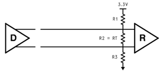
With that in mind I think it is possible to calculate the value of the external pullup and pulldown resistors to make the output low when the differential input is 0V.

Best regards,

Santiago

  • Santiago

    If you look at the Table 1, Truth table in the datasheet, you will have to actively drive the input such that the VID < -0.1V in order for the output to be low.

    Thanks

    David

  • Hello David, thanks for your response

    Yes, of course, We have to drive the input to change the failsafe output.

    But the selection of the resistors depend on the bias current desired, and this value must be small (less than the 3mA current of the LVDS signal when the driver is connected, so it does not affect the LVDS signal) but not smaller than the internal fail-safe bias (because the internal failsfe will be stronger than the external, and the added resistors will have zero effect).

    Do you have some information on internal failsafe bias current?

    Best regards,

    Santiago

  • Santiago

    I don't have the exact internal failsafe bias current information available. But looking at the datasheet, it seems we have internal 20mV – 10mV single ended. Given that the LVDS inherent 20mV noise margin, we expect RT to be 100 ohm while R1 and R3 are about 6.2K and 10.2K respectively. You should be able to verify this as well by shorting the pin or sourcing the current.

    Thanks

    David

  • Hello David,

    We do not have any DS90LV048A to measure and make some prototyping yet.

    And I am unable to find this in the datasheet:

    it seems we have internal 20mV – 10mV single ended

    Can you explain me how you get that, please?

    It think that it should be Vid=+35mV across RT, making VTH=-35mV and VTL=-35mV as shown in the Electrical Characteristics table.

    Thus I(RT)=350 uA , R1=5807 ohm and R3=3521 ohm. Were R1 and R3 are internal

    This makes sense to you?

    Thank you for your help,

    Santiago

  • Santiago

    I thought there is a mention of internal failsafe bias voltage of 10-20mV in the datasheet, but I can't find the information now.

    But I do not see an issue with your calculation.

    Thanks

    David