This thread has been locked.

If you have a related question, please click the "Ask a related question" button in the top right corner. The newly created question will be automatically linked to this question.

TPS25750EVM: USB-C PD solution request

Part Number: TPS25750EVM
Other Parts Discussed in Thread: TPS25750, BQ25792, TPS65987DDK

Hi Guys,

Good day. I'm posting this in behalf of our customer, kindly check the full details of the inquiry below. 

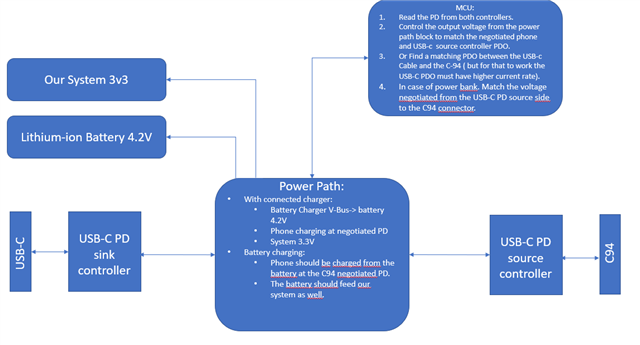
We are developing an intermediate phone- case that plugs to the phone from one side and the charger from another side through C94 iPhone lightning connector and USB-C cables.

Our case has many use one of them is to be a power bank . So we have a battery installed in our case which provide the phone with Power delivery fast charge, and on the other hand, we have to charge ourselves and the phone with power delivery ( if in charge mode) . So we are a middleman between the charger and the  phone in which we need to provide power delivery for our battery and the phone.

The main issue is that we are restricted to work with fast charger that comes with the phone and at the same time to provide proper PD to our system and the phone.

Restrictions we have :

  • Since PD is negotiable through CC line for specific voltage and current we must insure that the PDO coming from the charger has the same voltage and higher current value  than the PD of the phone ( higher value since we need to feed our system as well). 
  • The charger and the phone are made to work together so they have profiles that works together and by adding a power path to our system we might lead the charger to work over the current value negotiated for.
  • We cannot add any BUCK-BOOST voltage regulator to match the voltage (between the phone and the charger)  since we are restricted in the size of the PCB. (3A current and heat dissipation coming from other components)

What we need:

  1. We are working to find a way to read all the profile that the charger have and what the phone have.
  2. Based on (1) we will find if possible a matching profile where we have the same voltage but from the charger side a higher current rate.
  3. And always keep monitoring the voltage values between the charger or the phone so we can readjust the PDO whenever the external devices (phone or charger) chooses to change it.

 As for the communication we are restricted to work with an MCU  or if TI have a module that have in it a MCU+WIFI+(BLE5.0 >) .

If there are a solution for such request we will be very happy to hear it. 

Thank you in advance for your support. 

Best regards,

Jonathan

  • Jonathan,

    You should take a look at this reference design:  https://www.ti.com/tool/USB-PD-CHG-EVM-01

    They should be back in stock in the next few days.  This reference design implements exactly what you are describing in as small a formfactor as we are capable of producing.

    Regards,

    Chuck

  • Hi Chuck,

    Apologies for our late response and thank you for sharing the reference design, however, the proposed solution doesn't quite work with our customer but it answers half of what they need.

    Here is our customer's feedback :
    What we need is to have control over PD from two different side ( the charger side and the phone side in which both of them speaks using power delivery protocol simultaneously). We are looking for a solution that charge us as battery and simultaneously charge the phone through PD.


    The given method can help our battery to charge through PD from the charger side but don't control or negotiate the PD from the phone side ( the case is always connected to the phone from a lightning connector ) and have one access to the charger through a USB-c connector.
    The only problem is that the BQ can deliver a voltage power path to the phone through Vsys but don't the voltage to match the negotiated PD from the phone.

    So in our case we must need two TPS25750 one working as a sink from the charger side and another one working as a source from the phone side. The good news is that TPS25750 gives the host to read the charger PDO and the phone PDO but does it allow us to choose which PDO to work with ?

    And the solution might works with us if the BQ Vsys voltage is regulated through another Buck-Boost controller to regulate the voltage between both TPS25750 is such way we can achieve a good solution.
    So we what we are trying to do is to avoid adding another buck boost regulator between the TPS25750 chips. But we can allow to forget about the middle buck-boost converter if and only if we have full control of what PDO the TPS25750 have to allow as profiles ( just to match the voltages between the phone and the charger).

    Thank you for checking. 

    Best regards,

    Jonathan

  • Jonathan,

    Do the want each of the 2 ports to be able to be either a source or a sink?

    Do they have a high level block diagram of the individual blocks?

    I know that we have a variant of the 792 charger that has 2 inputs, so we can address getting power into the battery from either path that way, but we will have to build a power tree that will provide the output power desired from the battery to the DFP connector.

    This is a more complicated power structure, so I am asking some more detailed questions.

  • Hi Chuck, 

    In response to your questions. here is the customer's reply.


    1) Do the want each of the 2 ports to be able to be either a source or a sink?
    - No we do not have such requirement. From the charger side we need to have a Sink controller and from the lightning connector we need it to be a source controller.


    2)Do they have a high level block diagram of the individual blocks?
    -Yes, Kindly check the attached file

    Thank you for checking. 

    Best regards,

    Jonathan

  • Jonathan,

    The block diagram is very helpful.

    The TPS25750D is a good choice for this system from a USB C interface standpoint. 

    Let me describe how it would work for both situations  you have described.

    As a sink, it will allow for a fully autonomous interface that can be configured to act as a sink controller to allow any type C supported Voltage/Current input to the power tree.

    As a source, it has a few limitations. 

    1.  The TPS25750D only supports 5V Pd contracts when not using the Charger for the integrated power path, and I do not see a way to suppor this option in the current block diagram.

    2.  The TPS25750D requires that PP5V be supplied with a power source capable of providing at least 3.5A of continuous current
    3.  The TPS25750D requires that VIN_3V3 be supply with a 3.3V power supply (low current)

    Regards,

    Chuck

  • Hi Chuck,

    Here is the customer's feedback. 

    As mentioned in the datasheet of TPS25750D, if we negotiated a source contract we can only work with 5V (PP5V) voltage, but in the below document page 14
    www.ti.com/.../tiduey1.pdf
    It mentioned that sourcing 20 V with BQ25792 in OTG Mode through TPS25750D is doable and the sourced voltage was 20V, although the datasheet stated that when working in source mode the PPHV is disabled and also do you have any source controller chip recommendation where we can program its current and voltage profile (similar to TPS25750 but without its source limitations?)


    Best regards,

    Jonathan

  • Hi Chuck,

    Our customer just need to confirm point 2. 

    Here is the customer's update: 

    1)I think that regarding the last post i understood that soucing gonna be through the Vsys path of the BQ which is gonna feed the Vsys connector.
    2) As for sourcing limitation i found the tps65987ddk can help with the sourcing as well as the sink capabilities but need to confirm that we can read and write as well as controlling the pdo for sourcing and sinking application.

    Looking forward to your response. Thank you

    Best regards, 
    Jonathan

  • Jonathan,

    You will be able to read and write to the TPS65987DDH (The DDK is only for USB4.0 systems) and it can be controlled for both PDO source and sink applications.

    Regards,

    Chuck