Hi!
I'm trying to add timing constraints on the FPGA side, which is receiving RX data from the DP83822I PHY.
I'm going for 100Mbps.
Question 1:
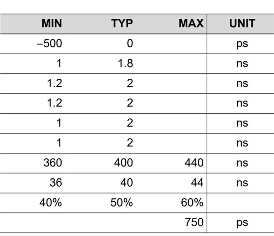
Figure 7-12 contains both SetupT and SetupR:
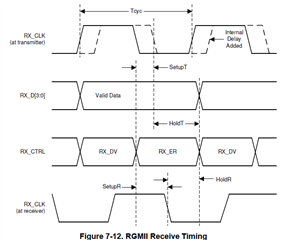
Why is both SetupT and SetupR in the figure?
Is SetupR/HoldR trying to describe the valid window at the FPGA (receiver)? (making assumptions about our PCB?)
Question 2:
(In chapter 7.16, the following is specified:
SetupR = min 1 ns,
HoldR = min 1 ns )
Based on SetupR and HoldR, it seems that the data valid window is only 1+1 = 2 ns, even though the clock period is 40 ns (for 100Mbps mode).
Did I interpret this correctly? It seems a bit narrow.
Question 3:
In the table for SetupR etc: since we constrain for worst-case, I assume that we should ignore the "TYP" column and only use the "MIN" column, right?