This thread has been locked.

If you have a related question, please click the "Ask a related question" button in the top right corner. The newly created question will be automatically linked to this question.

TPD4E001: Vcc pin can be open?

Part Number: TPD4E001
Other Parts Discussed in Thread: TPD4S012

Hi Experts,

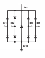
Below are block diagram of TPD4E001. It can clamp IO voltage. 

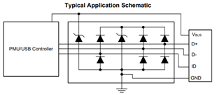
Below is another ESD device block diagram for TPD4S012.

It is very similar only other than Vcc pin of TPD4E001. If Vcc pin of TPD4E001 is left open, is it same function with TPD4S012? What does Vcc pin make difference between TPD4E001 and TPD4S012?

Regards,

Uchikoshi

  • Hi Uchikoshi,

    The Vcc pin on TPD4E001 is there to regulate the clamping performance of the IO pins. AS you can see, it is connected to the cathodes of the steering diodes of each IO pin. Therefore, if the voltage on the IO pins increase past the Vcc voltage, the current will start flowing through the Vcc line until Zener breakdown occurs, which is around 11 V. If the Vcc pin is left open, the device will only start conducting at the breakdown voltage. 

    For TPD4S012, the Vbus pin is completely separate from the other IO pins. It has a separate Zener diode with a higher breakdown voltage than the other IO pins. Therefore, if you leave the Vbus pin open, it will have no effect on the other IO pins. 

    Regards,

    Matt Smith