This thread has been locked.

If you have a related question, please click the "Ask a related question" button in the top right corner. The newly created question will be automatically linked to this question.

TCA9536: Unresponsive chip on new board

Part Number: TCA9536
Other Parts Discussed in Thread: TCA9617B, TMP175

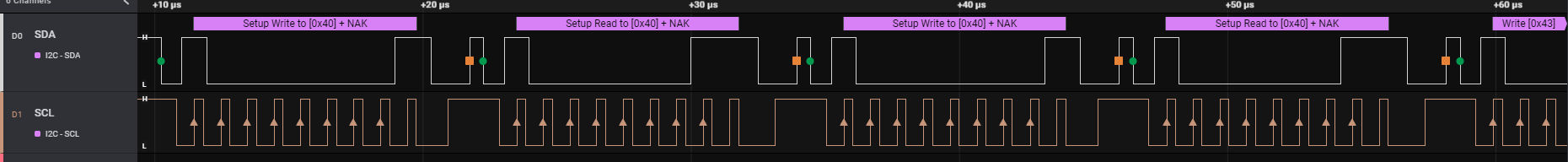
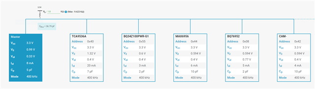
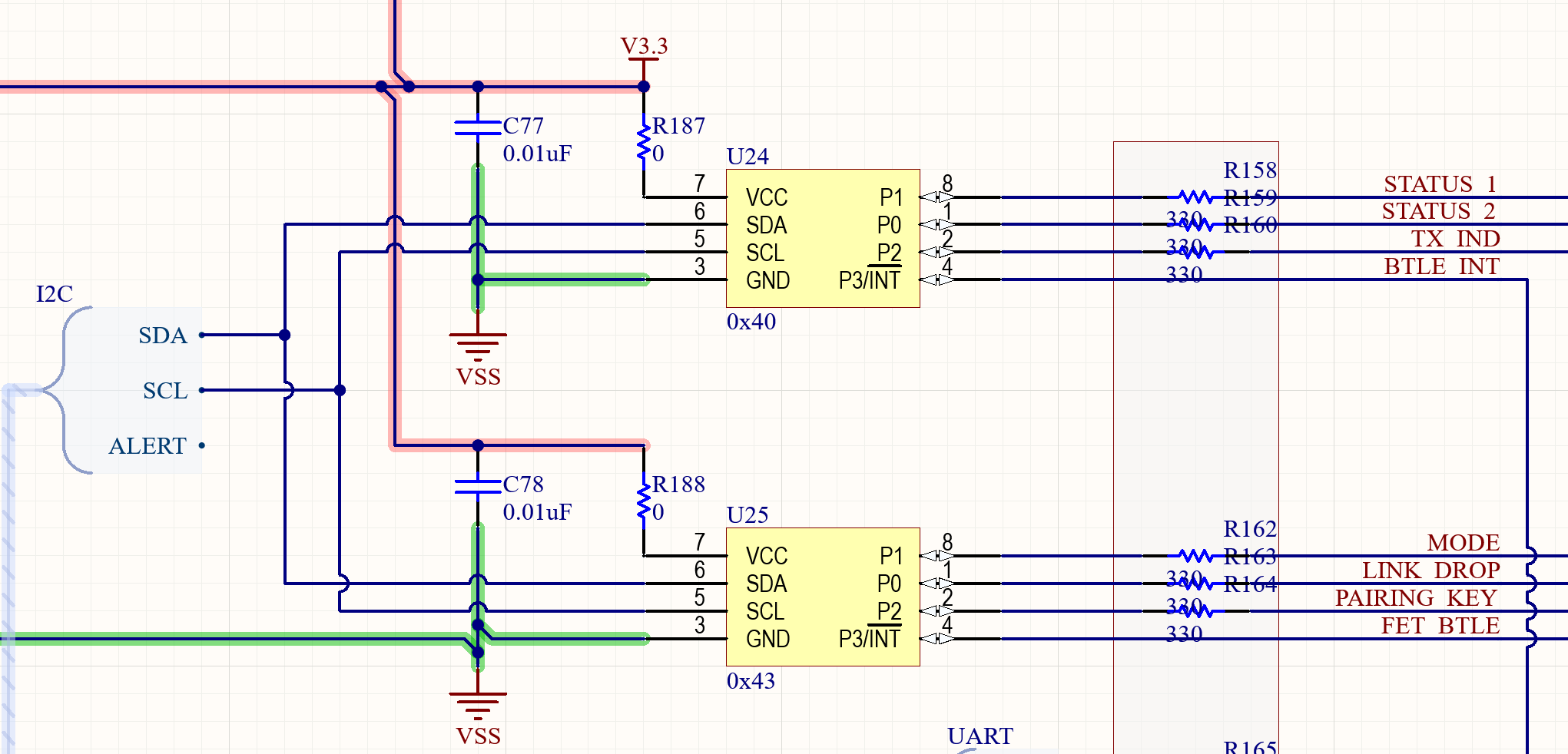
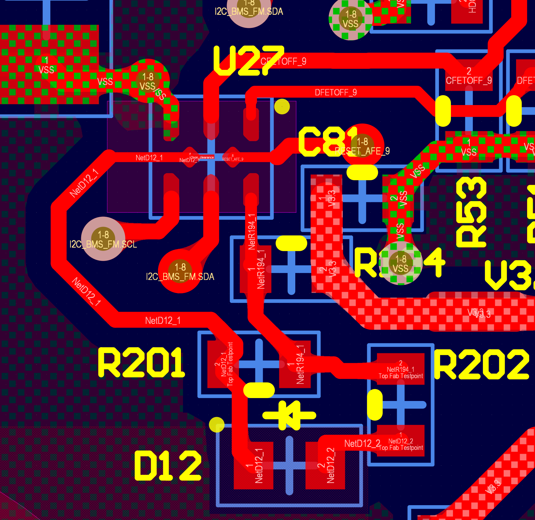
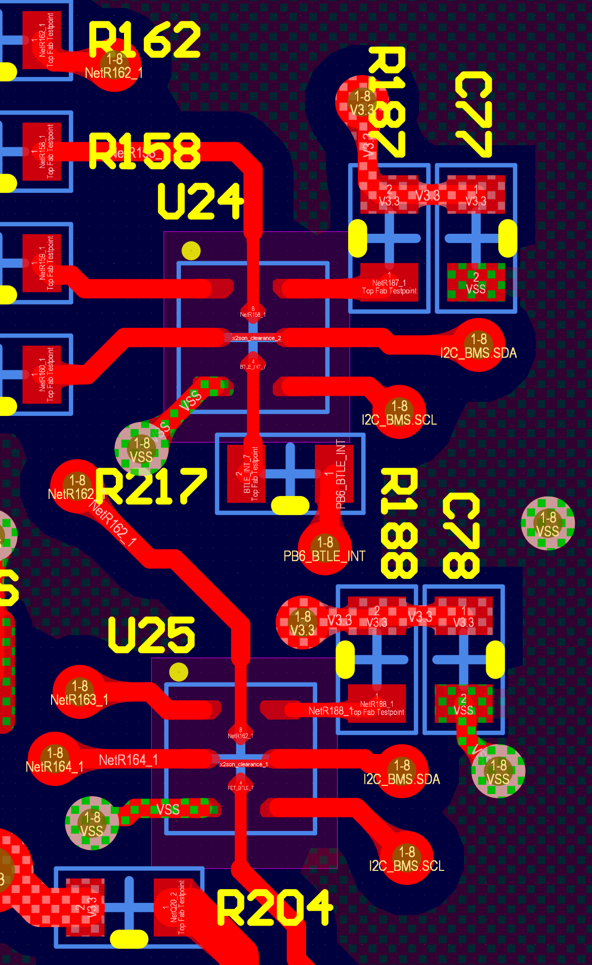
I have a TCA9536A and a TCA9536B right next to each other on the a FM+ bus. And I have another TCA9536A on a FM bus.

Quickly testing this prototype board I thought I was seeing communication from both the A and B on the FM+ bus; so I switched to bringing up the FM bus. But now I'm not seeing any communication from the A chip on the FM+ bus. It's possible it wasn't working the first time around.

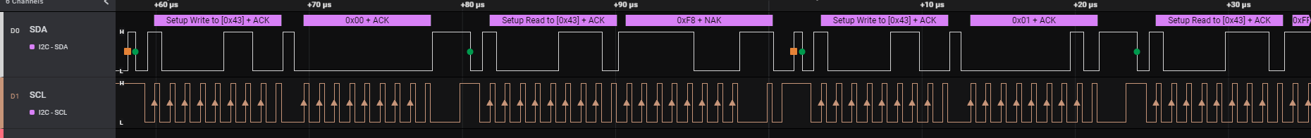
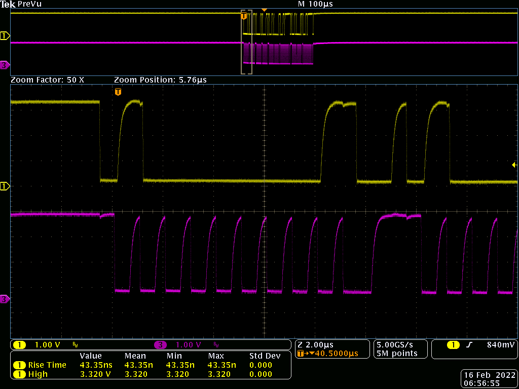
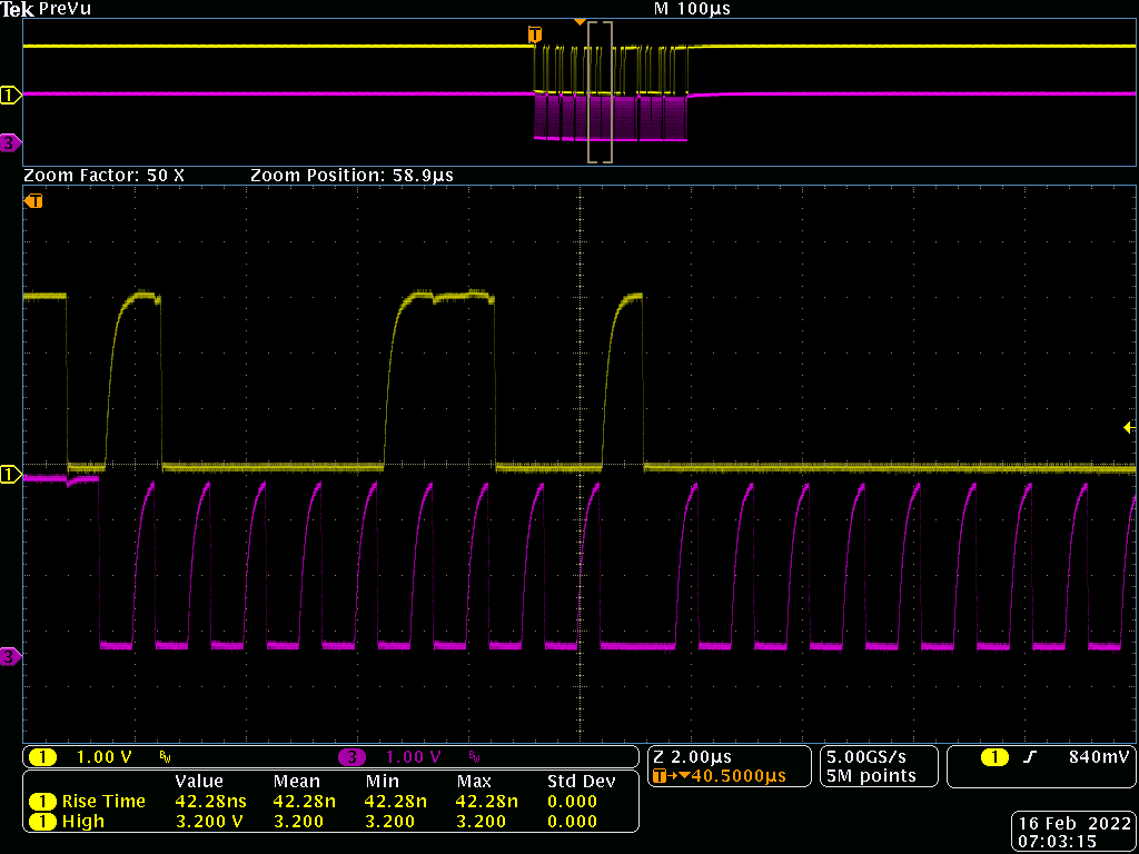
But could you help me determine what I need to look to get this going? The "B" is responding, and I've poured over all the i2c timing and it all looks good. 

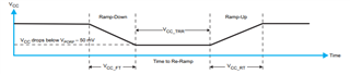
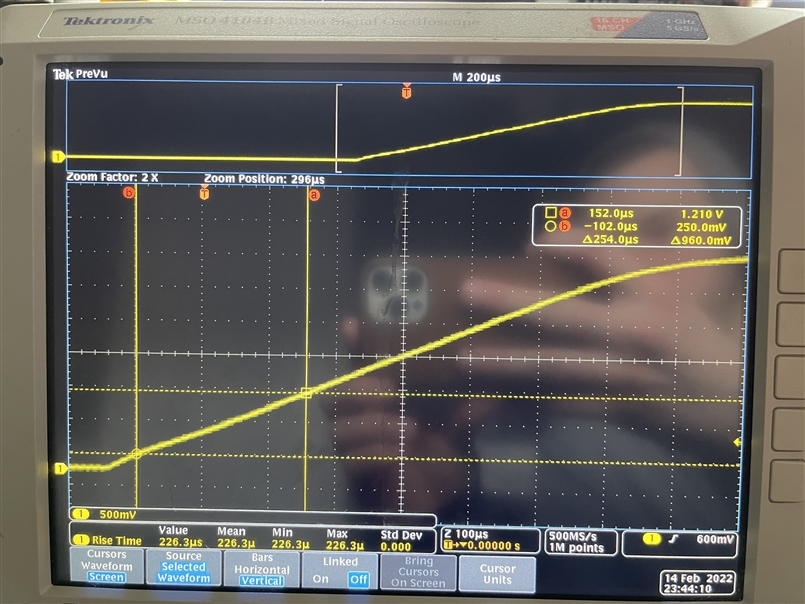
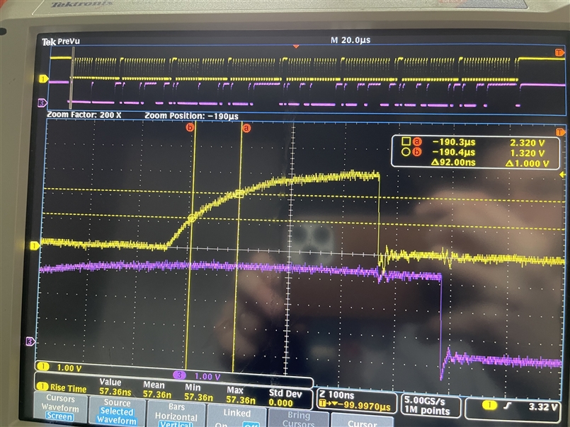
Regarding the power on ramp, what part am I needing to characterize? I'm not understanding the POR section as it doesn't clearly indicate what initial non-reset conditions should be. Vcc = 3.3V; it ramps from 0V to 1.65V in 424us, very linearly. 

  • Hi Jason,

    Can you include a block diagram of your setup so I can better visualize what it looks like?

    Just to confirm are you trying to have one FM+ (1Mhz) bus communicate with an FM (400kHz) bus, or are these two separate buses and you can't get the TCA9536 to communicate at the lower speed?

    Lastly, what test are you preforming to ensure that the A and B device on the FM+ bus are communicating properly?

    For the power on reset I am going to use the diagram below:

    First there is a minimum rise time (0.1 ms) and fall time (1ms) for the power on reset. The device has to be already power up to Vcc = 3.3V for a power on reset to occur. If you drop the voltage too fast or ramp it too fast a power on reset will not occur. The device also must be lowered to Vporf-50mv which for this device is a minimum of 0.75V-0.5V=0.25V.

    It might be that this device requires a power on reset before it enters normal operation:

    Best,

    Chris

  • Hi Chris,

    I have two individual buses. Both driven from an ATSAME51 ARM processor. One is operating at 1000 kHz, the other at 400 kHz.

    I'm not understanding the POR. Are you saying it is required that I droop the power line to 0.25V and bring it back up to 1.2V before the chip will even operate? I do not have the ability to droop the supply voltage.

    Here is the rise time from an initial power on from 0.25V to 1.2V it is 254 us.

    The FM bus has one TCA9536A which is operating properly.

    The FM+ bus has a TCA9536A and a TCA9536B, where only the 'B' chip is responding to its address. 

    I'm reading out the register values; for the responsive 'A" chip on the FM bus I have it successfully driving some IO.

    I'm using a logic analyzer to view the signals. 

    Here's a scope capture on the rise time of the FM+ clock right at the unresponsive IC. ~92 ns.

    I2C_FM:

    I2C_FM+

    'A' on FM bus

    'A' and 'B' on FM+ bus

  • Hi Jason,

    I'm looking at the block diagram for the FM+ bus and I don't see the second TCA9536A. I only see the TCA9536B:

    Where does it fall in this chain of devices? I assume it is in the second chain after the TCA9617B.

    Also do you know roughly what your bus capacitance is for each side of the TCA9617B, including the capacitance of your traces?

    I'm unsure if you sent this above but can you send me an oscope shot of the SDA and SCL signals when you try to perform a write to the TCA9536A on the FM+ bus? I mainly want to see the first byte where you send the address.

    You can also include an oscope shot of TCA9536B receiving a write just so I have reference for what is working.

    Best,

    Chris

  • Hi Chris,

    I accidentally deleted the ‘A’. They are both on the ‘A’ side of the buffer. The buffer is actually an NXP PCA9617. The only devices on the ‘B’ side of the buffer are the TMP175’s in the diagram and I’ve tested them all. 

    I didn’t see any response regarding my power ramp. Can you tell me if it is required that I perform a power on reset before the device is functional? Can you also tell me the the startup power ramp needs to look like? 

  • Hi Jason,

    Regarding the POR, a POR is required to occur for the device to function normally. However, this will happen automatically as long as your ramp up times are within spec. For your setup 254us is within spec so you should be fine. I don't think a POR is your problem.

    Just for your benefit I'll explain how to achieve a POR. The POR looks like this diagram:

    After the device is powered on and reach VCC, you ramp it down to at least 0.25V (V_PORF-50mV). The fall time of this ramp down must take at minimum 1ms. If the fall time is any faster the device will not recognize it as a POR. After the ramp down the VCC rail must be held at 0.25V or below for at least 2us. Then VCC can be ramped back up to the normal VCC level. The rise time must be at minimum 0.1 ms. Let me know if you have any other questions about POR.

    Were you able to get any oscope shots of the communication between the Controller and the TCA9536A?

    Can you also attach some photos of the device soldered into the PCB? I would like to check the top side markings of the device and the orientation on the PCB.

    We can continue debugging from there.

    Best,

    Chris

  • Here is the i2c addressing 0x40 right at the chip.

    Here is 0x43 for U25 right next to it.

    The printing on the chips isn't really visible, even with a little magnification, and I don't have a microscope here. We had the assembly house run X-ray on the remaining qty of our prototype run and they saw no evidence of solder bridging, and confirmed correct operation of the IC's on those boards. Knowing the pin 1 indicator is a corner bracket, these both appear correct.

    Here is the 'A' IC from the slower bus; markings on it are more clear

    Here is a capture from a different board under microscope. Note that the only board testing has been done on is the one I have, not this one. I will have another board to test Friday.

  • The IO pins on the IC in question are connected to bluetooth module. There is no power to that IC, but it seems like its inputs were not high-Z and there was some impedance between them and VSS. Voltage levels between the bluetooth module and the TCA9536 therefore were around 1V. I removed R158, R159, R160 (see schematic above) and the output voltage at the TCA9536 was then correctly 3.3V. So I think the chip is populated in the proper orientation. 

  • From what I can see everything looks correct. The top markings indicate that the A and B version were used. The orientation of the chips looks correct.

    For the scope shots the time it takes to go from 0.3*VCC to 0.7*VCC should be 120 ns or less for FM+. On your scope shots I can't really tell what your time/div is. I do see a rise time of 42ns but you verify that this is the case.

    For the next steps can you check the VCC of the device that is not working. Make sure that it is receiving 3.3V.

    Then can you take the known working TCA9536A on the FM bus and switch it with the TCA9536A on the FM+ bus. Let me know if switching the device fixed it. I can't make out what the marking on the TCA9536A on the FM bus is. The marking should be 1IR. Can you verify this for me?

    Best,

    Chris

  • Chris,

    I supplied a capture of the 3.3V supply two days ago showing the power on ramp. And yesterday I noted that the output of the TCA9536A is at 3.3V indicating the internal gate and pull-up of the IC are operating properly.

    SCL rise time is 90 ns. 

    Are you suggesting that I try desoldering an X2SON? I don't think I will be able to do that; I do not have a hot air rework gun. I also don't want to remove the functional IC.

    The images you see attached are the clearest that I can see as well. For the unit I have in front of me I can't discern anything on the IC. The image from my coworker with the other board clearly shows 1IR for the 'B' package. But the 'A' package looks more like it says 1IS or 1I5. The 'A' chip on the FM bus clearly says 1IR.

  • Thank you for clarifying the marking should be 1IR; I have been incorrectly inspecting the lower IC, which is in fact the 'B' device. Of course VCC, SDA, SCL are all presenting as identical since they are so close, and I've measured at both, but I will now try and look at the outputs of the upper IC as well.

  • I pulled all the series resistors to the IO pins with no success. Probing the solder joints themselves with a fine tip lead caused the IC to become functional. Once I added back in the resistors I lost functionality again. I tried touching the joints with a fine solder tip to reflow them, but had no effect. I can press down on the IC and get it to work. I think there is definitely a cold joint somewhere.

    We are using these on a 2 oz board. Is there anything specific we can have our board house look for in their process for these? The footprint is built to the TI drawing. The TI drawing calls out 0.0325 mm solder mask expansion; we are at 0.05mm

  • Hi Jason,

    The only thing the Datasheet offers for the process of soldering this chip is a solder paste example:

    They specifically say :Laser cutting apertures with trapezoidal walls and rounded corners may offer better paste release. IPC-7525 may have alternate design recommendations.

    I'm looking at the footprint on the Altium images you sent. There isn't a trace from SDA to P2 right? It looks like a trace from this distance but I can't tell what it is.

    Best,

    Chris