This thread has been locked.

If you have a related question, please click the "Ask a related question" button in the top right corner. The newly created question will be automatically linked to this question.

SN65HVD24: SN65HVD24

Part Number: SN65HVD24

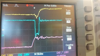
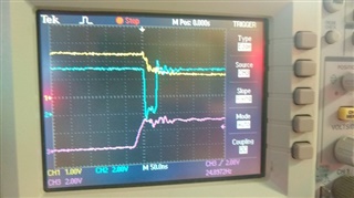
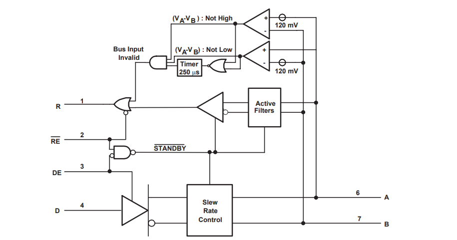
We are trying to use the SN65HVD24D in our application (in place for example of Exar XR33055 or Maxim MAX33071EASA+) but it fails due to UART errors. The speed is only 1Mbps, and the bus does have external biasing. I suspect the reason is a glitch seen on the output when Transmit enable is set high (the /ReceiveEnable is low). The glitch is short (only around 40ns) but since the UART reports noise errors, I think it is a problem.

Have you seen this glitch before?

  • Hi Mark,

    Can you possibly share a scope shot of both the Transmit Enable signal and the output at A/B (or the the differential voltage between A and B is also fine) Labeled with max/min voltages would be very helpful as well. I would like to know a little bit more about what the glitch is looking like so I can see if I can diagnose the phenomena that is being seen. There is a propagation delay that is 25ns - 50ns long (typ - max) - while I don't necessarily think this is what is being seen I just want to double check.

    Also have you seen this phenomena on multiple IC's ? 

    Also what is the rise time on the enable signal and is there any delay intentionally added to this line- as logic pins regardless of IC can have some strange effects if the rise time is too slow - it usually isn't an issue (hence why you usually don't see it mentioned on newer parts), but it could possibly cause a glitch if that rise time is too slow. As a lower impedance path from VCC to Ground can form and cause some VCC dips or other effects - the circuits are shown below

    Please let me know and if you can attach scope shots that would be very helpful so I can start digging into the possible causes. As a glitch may have multiple root causes and I just want to start looking at which ones we can eliminate. 

    Best,

    Parker Dodson

  • The glitch is not seen on equivalent Exar or Maxim parts in the same circuit.

    The Transmit enable (pin 3) edge is not slow, rise time is about 30ns.

    Attached are a couple of photos of oscilloscope measurements. Pink is Tx Enable, blue is the Receive output (pin 1) with the glitch (Receive enable is permanently logic low). Yellow is the output: pin 6 'A' is the one that goes high but first glitches briefly low. The second plot with pin 7 'B' just goes low without a glitch. The problem is pin 6 going slightly low for about 40ns before it goes high.

    We think that although our code doesn't 'listen' to the outgoing message, the connection of the Receive (pin 1) to the UART is probably causing a UART error based on the STM32 processor's standard UART settings, and our code disconnects the device if there are too many UART errors.

  • Hi Mark,

    Thanks for the additional information.

    I should have a few of these parts in our lab that I can run some tests to see if I can duplicate the results for the application (in terms of the glitch because I agree that the UART errors being thrown could cause the system to disconnect). 

    To confirm I am running a similar test could you confirm the following:

    1. VCC voltage used

    2. Confirm if the DE and /RE pins are shorted together

    3. Are there any passives attached to the R pin such as resistors or capacitors - if yes how are the connected - if no I'll assume just a high impedance load/open for testing. 

    4. Are there pull-ups or pull-downs on the A or B pins.

    5. Are you using  termination and if so what is the value.

    Also could you confirm if this issue has been seen across more than 1 unit?

    Please let me know - so I can test some of these parts in lab and see if I am getting similar results and if I am not  we can go from there to see what differences between my setup and the application that could be causing this issue. 

    Best,

    Parker Dodson

  • 1. VCC is 5V

    2. DE and /RE are not shorted together. /RE is permanently at 0V. I expect if /RE and DE were shorted together, presumably the glitch would not occur, because the Receive would be disabled just before the glitch. DE is the trace shown going high, which triggers the glitch.

    3. No, there are no passives on the R pin. I have also temporarily tried an RC filter on the R pin to filter out the glitch, but although it seemed to reduce the problem it did not remove it: it looks like when the filter is large enough to squash the glitch, the edges are too slow to avoid UART errors anyway.

    4. Yes there is biasing on the A and B pins (both ends of the link): pin 6 3k3 to 5V, pin 7 3k3 to 0V. Some ports are 1K5 instead.

    5. Yes there is 120R termination at both ends.

    Yes we see this issue on multiple Texas ICs and also on 3 different date codes we were able to try.

  • I tried our system with /RE shorted to DE (instead of /RE to 0V) and although the glitch when DE goes high has gone, the system still does not work (still due to UART errors). I think it is because there is now a 1us glitch on the Receive input when the /RE+DE signal goes low! This one is not related to any glitch on the A or B pins. Almost as if there is a triggering of standby due to the transition? Anyway, it doesn't look as if connecting /RE to DE in our design is able to help us.

  • Hi Mark,

    First off - I'd like to apologize the units I had have been repurposed so I didn't have material to test today - that being said I have new units on the way and they should be here Friday   - so I can test Friday or Monday depending on when I receive the parts. Once again I am truly sorry as I had units about a week ago and thought I still did. 

    That being said - with the information you did provide - I think I know what may be happening. So since /RE is always held  low - the receiver never shuts off - if you could clarify where the 1.5k Ohm resistors are as these resistors along with the 3.3k set the idle bus voltage - when the device starts to transmit the A/B signals start - by the scope shots you have taken it seems that "B" could possibly be greater than "A" for a brief period of time - which may be causing the device to register a logic 0 before A and B go back to a logical 1 state. 

    A possible solution that could be implemented is to increase the pull ups/ pull-downs strength - (if there are 2 VCC pull ups and 2 GND Pull-downs if they all take the value of 1k to 1.2k you will get a higher bus idle voltage that may be more immune to the start up signal that could prevent the glitch.

    Or another solution would be to implement a delay between the application of the "DE" signal and the Data signal on D. If DE/ /RE are shorted together this will allow time for the receiver (R) to shut off  - if a high signal is needed on this pin using a pull-up could help here so that when R goes high Z its still a logic high value on this pin. I'd also still implement stronger pull-ups/pull-down fail safe resistors on A and B (you don't need them on both sides of the line - only 1 side - but if 2 sides are used you should use the 1k to 1.2k - if only one side is used half the resistor values to 500 to 600 Ohms) - this ensures that that bus idle voltage is above threshold and R will output high until it goes high Z - which the pull-up on that line could help. 

    Please let me know if this modification is possible (and if it is - see if you are better off) , as well as the location of the 1.5 K ohm resistor (this is so if I need to recalculate the fail-safe values I can). When I receive the parts I can also perform this test and report back by Friday or Monday depending on when I get the IC's in to test - but I will keep you updated. I apologize for the delay once again - but I do think the problem is that when the /RE pin is always low the idle differential bus voltage could be close to threshold and during the first transition could cause the small bump on B over A to cause brief logic 0 output - seen as the glitch - if the fail safe resistors are slightly stronger this may improve the noise sensitivity of the device and this glitch could possibly be mitigated.

    Best,

    Parker Dodson

  • I can't agree that there is any likely benefit from these points. Because of the 60R overall resistance between A and B (120R each end) the bias resistors of 3k3 (assuming same each end) only contribute about 70mV of bias voltage, which itself should not even be needed because the receiver is 'failsafe'. Given the 40ns glitch seems to be about 400mV in size, I expect the glitch to defeat any practical value of external biasing. The maximum level of biasing is limited in our design by the size of resistors used, and their possible dissipation in some circumstances. The biasing is in the right direction, i.e. pin 6 'A' upwards, and pin 7 'B' downwards.

    The R pin does already have a pullup (to 3V3). When /RE is tied to DE, the 'high' value of R goes from 5V when /RE is low, to 3V3 when /RE is high, as expected. But both levels are a logic 'high' to the receiving UART.

    Also a long delay from DE high to first D signal is already present. But the problem pulse on R is not at the time DE goes high: behaviour is OK then (the 40ns glitch has gone). With DE and /RE connected together, the 1us pulse on R is present straight after DE and /RE go LOW, and without any such pulse appearing on the D signal or on the external A and B pins. That's why I suspect that /RE going low is taking time (about 1us) to exit an internal standby state on the receiver, and the R output is low until the standby condition is cleared? If not and it is a biasing issue, why consistently 1us long? Halving the value of the biasing resistors would be possible, but do we really think that is necessary on a chip with failsafe operation included?

  • Hi Mark,

    The failsafe thresholds take 250us to respond. Until that time is reach the normal thresholds are used - which are 60mV and -60mV typical. 

    At 70mV you are slightly above typical for the positive going - but this threshold could be higher (up to 200mV) and at the startup when R is still listening there is a change in the voltage which is shown in the scope shots you provided could throw the threshold into the negative threshold range. I can't tell an exact value because A and B are on different shots. Increasing the strength of those pull-ups could lift the idle voltage and the swing at the beginning could be rejected. Is this a guaranteed fix - no, but its a generally simple modification that could prevent a "0" even falsely being read by keeping the idle bus voltage at or slightly above 200mV so it remains high during that initial startup signal where the problem seems to be seen. This is something I will be exploring as well when I get parts in - I expect them in today. 

    With all that being said - on the point when you tie /RE and DE together and there being a delay during this delay it is pulling down. So after looking a bit closer - yeah that is expected. There is a max time of 2us (we don't spec typical - so a 1us isn't unrealistic) - essentially when the /RE pin goes high there is a period of a max of 2us for the device to go High Z - I am not sure why this is pulling down during this time - but it could be just how the circuit behaves during the transition. 

    That being said:

    R is going low when you don't want it to. This means the Bus invalid input is low, and depending the scenario the active filter is also giving a low value. From the diagram above you can see there isn't many pathways that affect the R output in normal devices - and judging by the tests you have done I do think these are standard devices - they don't seem too be damaged. 

    In the first case the receiver is always enabled - the bus invalid failsafe will not force a high on the R pin for 250us. During startup there could be a period where a logic 0 can be produced. The reason I am leaning towards this being a possible bias issue is that the bias voltage while probably ok in most situations during start-up this could be too little bias for the actual device (will come back with confirmation when I receive parts on this) and since the same problem is being seen across lots I doubt its damage to the part. 

    In the second scenario - There is transition time - but I am unsure why its pulling down it should be transitioning to Hi-Z - but it is something that I will also see if I can repeat in lab. 

    As I mentioned a couple days ago - I do have parts expected today - hopefully afternoon and I should be able to get data by next Monday (barring any delays in the part delivery) and I will be testing this scenario trying to 1. recreate your issue seen and 2. if problem is repeated I will then adjust biasing resistors and see if any resolution is possible by strengthening the bias, 3. if that fails I will just see what other tests I can do to try to pin-point what is happening from the receiver side.  

    I will have an update for you Monday to inform you of my progress.

    If you have any other questions in the meantime please let me know and I will see what I can do.

    Best,

    Parker Dodson