Because of the Thanksgiving holiday in the U.S., TI E2E™ design support forum responses may be delayed from November 25 through December 2. Thank you for your patience.

This thread has been locked.

If you have a related question, please click the "Ask a related question" button in the top right corner. The newly created question will be automatically linked to this question.

SN65C1168E-SEP: Vcc=0 initial condition

Genius 9880 points
Part Number: SN65C1168E-SEP

Hi,

For this IC, can customer applied input voltage when there is no Vcc?

For example, 5V at input of driver before voltage is applied to Vcc. If this possible, what is the maximum input voltage is allowed, it is the same as the recommended operating condition which is 5.5V? 

Thank you in advance.

Regards,
Maynard

  • Hi Maynard,

    The device will operate as spec'd when following the recommended operating table.

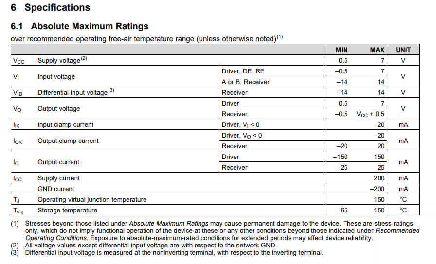
    To prevent damage to the part the maximum ratings should be followed:

    Based on the above table a few things can be found:

    1. The abs max differential input voltage (A - B) is  +/-14V , the min | max input voltage (DE, RE, Driver) -0.5V | 7V. 

    2. There are clamping diodes on the input pins (Driver, DE, and RE) from ground to input (input clamp current conditions is only for Vi < 0V). If input voltage drops below 0V the clamp current needs to be followed (-20mA) 

    3. The Receiver (R) has clamping diodes from VCC to R and R to GND as the max output of this pin is gated by VCC + 0.5V and it has a positive and negative clamp current rating. If the R pin goes out of range the clamp current (+/-20mA) must be followed.

    4. According to note 1 extended exposure to max rated conditions can affect device reliability and the device is not guaranteed functional at this point.

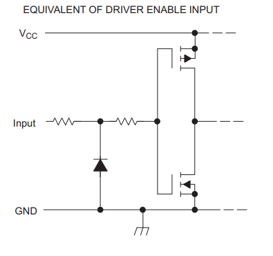
    With respect to your direct question - it shouldn't be that much of a problem to have a 5V signal on the D pin before VCC comes live as there isn't any ESD clamping to VCC on this pin so the part shouldn't sustain damage and with no voltage the logic input circuit shouldn't really react in a way that should cause too much risk to the schematic:

    The input structure is high impedance and shouldn't pass a signal when VCC = 0V. So it should be okay - but it as mentioned in note one of the abs max table is that extended exposure to abs rated conditions could degrade device reliability.

    Please let me know if you have any other questions!

    Best,

    Parker Dodson

  • Thank you Parker.

    Fernando