This thread has been locked.

If you have a related question, please click the "Ask a related question" button in the top right corner. The newly created question will be automatically linked to this question.

TCAN1042V-Q1: Schematic & Layout review

Part Number: TCAN1042V-Q1

Hi Team,

There is a good new that we DIN TCAN1042VDRBRQ1

And there have one thing need your support!
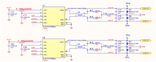
Please help check this SCH & layout, THX (please refer to attachment )

Layout.pptx

  • Hi Kygo,

    Here is my schematic review: 

    • Pinout on schematic matches pinout on datasheet: Correct
    • Decoupling included and valued well: Correct, we recommend an addition 4.7uf capacitor be placed near the VCC pin.
    • The STB pin on this device is active high. Internally the pin is pulled up to VIO so if you leave this pin floating and are not driving this pin the device will be in standby mode. If you want the pin to default to normal mode I would add a pull down resistor to this pin.
    • Everything else on the transceiver seems fine

    CAN Bus

    • CMC included and valued well: Correct
    • Termination resistors included and valued well: Correct
    • Split capacitor included and valued well: Correct
    • Filter caps included and valued well: Correct,  this value is a little high but depending on the number of nodes you have on the bus this is probably fine. Just make sure that you don't overload the bus.
    • TVS diodes included: Correct

    Layout

    • Can you send me the altium project to my email c-ayoub@ti.com It is not opening well through the power point. If you can just export the project and send the whole thing as a zip file to me.

    Best,

    Chris