


Other Parts Discussed in Thread: SN65LVDS31-33EVM
Hi,
I am working with Laurier and Aki on the linked issue.
In summary, we are trying to use the SN65LVDS33 to receive qty two 100 MHz clock signals (when I say 100 MHz, I mean a square wave signal with period of 10ns. Sometimes this would be referred to as 200 Mbps). Eventually we may move up to qty four signals, but we're just trying to get two working on the moment
The issue I am seeing is that when the phase of the two input signals is similar, the output begins to behave erratically: input transitions are missed, runts are seen on the output, etc. The issue seems to be aggravated at high temperatures. I've experienced the issue both on our custom hardware and on the SN65LVDS31-33EVM evaluation module.
My questions for the TI team:
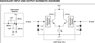
1. could DC-balancing be playing a role in the problem we are seeing? Is DC-balancing critical for this part? When I say "DC-balancing" I mean having an input signal that is roughly equally high or low, such as an 8b/10b encoded signal. I do see in the datasheet that although the device is NOT AC-coupled, there is an "attenuation network" at the inputs (internal to the part). It looks like the attenuation network sets up the biasing for a differential amplifier, so a non-DC-balanced signal will change this biasing. Currently, the clock signals I am feeding in have a duty cycle of 70%-80% (in other words, non-DC-balanced). Could such a "non-DC balanced" signal cause issues with the biasing inside the part?
2. I am looking at the output plots in the datasheet, and I see that the magnitude of the output signal is only about 400 mV. Why is this?
Thanks for your time!
