


Other Parts Discussed in Thread: TXS0102, LSF0102, TCA9406
Hi Team,
I have a few questions about this device.
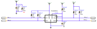
1. VCC1=1.2V or 1.8V and VCC2 = 3.3V. VCC1 will rise later than VCC2. What will be the behavior of SCL2 and SDA2 during this time? Will they be High -Z ? Will they Interfere with other communications running on I2C bus (The Bus SCL2 -SDA2 Connected to)? Reference schematic below.
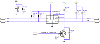
2. the same condition as above, and want to disable the SCL2/SDA2 connection using the DISABLE_I2C_CONNECTION. Will there be any problem since it will violate VREF2> VREF1 constraint given in the Datasheet when DISABLE_I2C_CONNECTION is HIGH? What will be the behavior of SCL2 and SDA2 during the time DISABLE_I2C_CONNECTION is HIGH assuming VCC1 is available during this period? Will they be High -Z ? Will they Interfere with other communications running on I2C bus (The Bus SCL2 -SDA2 Connected to)?
3. What is the difference between PCA9306 and TXS0102 devices? Is there a constraint for using LSF0102 instead of TXS0102 for I2C and PMBus? Both devices has auto direction sensing is there a constraint on maksimim- minimum external resistance to GND/VCC for those devices?
Regards,
Marvin

