This thread has been locked.

If you have a related question, please click the "Ask a related question" button in the top right corner. The newly created question will be automatically linked to this question.

SN65HVD1050: thermal resistance

Part Number: SN65HVD1050
Other Parts Discussed in Thread: ISO7760, ISO6760, TCAN1051H, TCAN1057A-Q1, TCAN1051, TCAN1051H-Q1, TCAN1051-Q1

Hi team,

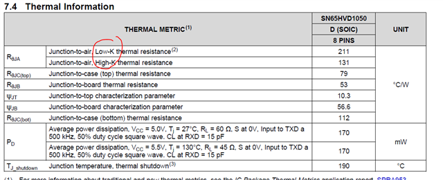
may I know what's the difference between low-K and high-K

my customer don't know which to use to calculate thermal.

is normal FR4 PCB belongs to low-K?

  • Hi Fred,

    Thanks for posting. This refers to two different JESD standards for thermal metrics: JESD 51-7 vs. JESD 51-3. These define different standards of effective thermal conductivity to the environment. Put more simply, they assume the air around the chip is different. More convective air will have higher thermal conductivity.

    The JESD 51-3 standard was defined originally and assumes that there is very little thermal dissipation availability. This is 1s or 1s0p analysis, meaning single signal layer, zero power plane. This is given above as "Low-K" thermal resistance.

    The JESD 51-7 standard gives more realistic environmental conditions that represent the real world. This is 2s2p analysis, meaning double signal layer, double buried power plane. This is given as "High-K" thermal resistance. This can result in as much as a 50% variation in RθJA as you see above.

    I recommend checking out SPRA953 Semiconductor and IC Package Thermal Metrics - particularly the "Test Card Impact" section, which describes this most directly.

    Best,

    Danny

  • Hi Danny,

    1. in short , JESD 51-3 is one layer, and JESD 51-7 is four layer, right? 

    2. may I know why they add a diode at RX?

    is it needed?

  • Fred,

    Edit: Yes, this would be a simpler way to think about it.

    Interesting, to me it looks like they're trying to implement some capability for voltage translation. In this case it's not needed, since both the transceiver and the MCU operate using 5 V logic. Alternatively, they could be protecting against some situation where B4 from U305 might pull low while RXD from SN65HVD1050 is high.

    I would not necessarily recommend having something on this path. The loop delay in a CAN node is relevant to its operation and communication, so adding this additional item would potentially add delay, effectively reducing your achievable communication rate. It is still workable if they're not reaching potential maximum data speeds, but if they start seeing bit errors in communication, this would be my first suspicion.

    Do they have a 3.3 V MCU that is pin-to-pin they're thinking they might add here?

    My recommendation is to drop D302 and R385 and replace them with 0 Ω resistors or just nothing. Also, the pull-up resistor on RX (R302) wouldn't be needed since the output of SN65HVD1050 is push-pull. The pull-up resistor on TXD (R301) would only be needed if the output B3 from U305 is open-drain.

    Regarding the U305 socket, have they considered ISO6760 or ISO7760 here in place of SI8663BD-B-IS?

    Best,

    Danny

  • Hi Danny,

    thanks for all the comment, yes I've promoted ISO7760 as p2p solution.

    since I know SN65HVD1050 may be not the new part,

    would you recommend a newer part that is BOMtoBOM or p2p to SN65HVD1050?

    for example, TCAN1051H?

    please also let me know the difference or upgrade of that part from SN65HVD1050.

    Happy new year

  • Fred,

    The SN65HVD1050 has an output VREF on pin 5 which serves the function of a SPLIT pin. In modern applications, this is not needed. If the customer does not need the output from pin 5, then the best upgrade would be the TCAN1057A-Q1. I would suggest that this is likely viable unless the customer is using the pin 5 output in a different/unusual way. Here is another E2E post that addresses the SPLIT functionality: https://e2e.ti.com/support/interface-group/interface/f/interface-forum/840892/faq-can-transceiver-split-pin

    Best,

    Danny

  • Hi Danny,

    so any SN65 old part come with this split pin , and new TCAN don't need this anymore, got it

    1.may i know what's the difference between TCAN1057 and TCAN1051?

    bus protection range?

    2. if the pin5 is NC now, can it replace SN65HVD1050 without changing schematic or layout?

  • Fred,

    The TCAN1057A-Q1 is the p2p upgrade to the TCAN1051H and TCAN1051-Q1 series. Yes, your note about the bus fault protection is correct - the older TCAN1051H and TCAN1051H-Q1 had the capability for ±70 V bus fault protection on CANH/CANL, however this is usually not necessary. In almost all systems, load dump is clamped below this. For 12 V systems, this is traditionally clamped at 40 V. In 24 V systems, this is usually clamped around 58 V. You'll notice that our newer devices support bus fault protection for ±58 V.

    For the pin 5 connection, the NC indicates that there is no internal connection to the IC; it is just the metal lead. However, you should take care to make sure nothing from the user's system was relying on pin 5, since this was originally an output from the SN65HVD1050.

    Best,

    Danny

  • Hi Danny,

    they use as typical way, I assume it's ok to drop-in replace, right?

  • Fred,

    As long as they are not using the V-version of the TCAN105x-Q1 devices, it will be a drop-in replacement. The non-V versions have a true no connect at pin 5, meaning that it will have no effect on the device regardless of what signal is connected to it.

    Regards,

    Eric Hackett

  • Fred,

    Yes, exactly. As Eric mentioned, pin 5 (for non-V devices) will just become an open connection like the right side of the diagram you included at the end of your last post ("TCANxxx"). This will be no issue for the TCAN1057A-Q1 to have this connection there.

    Best,

    Danny