Other Parts Discussed in Thread: MSP-EXP430FR5994, TCAN4550
I have a modified version of the TCAN demo working with MSP-EXP430FR5994 and TCAN4550 EVM. I can see the CAN packets on the PCAN analyzer.
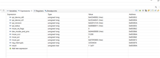
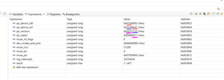
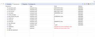
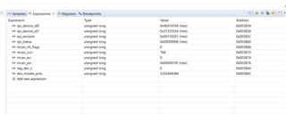
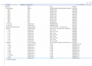
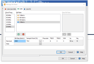
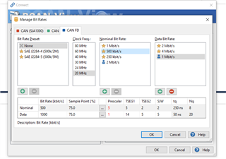
The custom PCB has a TCAN4551 chip and a 20MHz oscillator. I need help setting up the TCAN registers and the PCAN analyzer settings because the same demo project does not generate CAN packets on the PCAN analyzer. The CAN SPI CLK is 2MHz. Does this mean the CAN bit rate is 2kbps? Pasted below are my settings in the PCAN analyzer.
I did try changing the CLK_REF in the device configuration to 0, but nothing changed.
The existing production PCB also uses a 20 MHz crystal to the TCAN chip. Here is how to TCAN driver is setup in this project:
TCAN4x5x_Device_ClearSPIERR(); // Clear any SPI ERR flags that might be set as a result of our pin mux changing during MCU startup
/* Step one attempt to clear all interrupts */
TCAN4x5x_Device_Interrupt_Enable dev_ie = {
.word = 0x0UL
};
TCAN4x5x_Device_ConfigureInterruptEnable(&dev_ie); // Disable all non-MCAN related interrupts for simplicity
TCAN4x5x_Device_Interrupts dev_ir = {
.word = 0x0UL
}; // Setup a new MCAN IR object for easy interrupt checking
TCAN4x5x_Device_ReadInterrupts(&dev_ir); // Request that the struct be updated with current DEVICE (not MCAN) interrupt values
// If the Power On interrupt flag is set
if (dev_ir.PWRON) {
TCAN4x5x_Device_ClearInterrupts(&dev_ir); // Clear it because if it's not cleared within ~4 minutes, it goes to sleep
}
/* Configure the CAN bus speeds */
TCAN4x5x_MCAN_Nominal_Timing_Simple TCANNomTiming = {
.NominalBitRatePrescaler = 1,
.NominalTqBeforeSamplePoint = 32,
.NominalTqAfterSamplePoint = 8
}; // 500k arbitration with a 20 MHz crystal ((20E6 / 2) / (32 + 8) = 500E3)
TCAN4x5x_MCAN_Data_Timing_Simple TCANDataTiming = {
.DataBitRatePrescaler = 1,
.DataTqBeforeSamplePoint = 15,
.DataTqAfterSamplePoint = 5
}; // 1 Mbps CAN FD with a 40 MHz crystal (40E6 / (15 + 5) = 2E6)
/* Configure the MCAN core settings */
TCAN4x5x_MCAN_CCCR_Config cccrConfig = {
.FDOE = FDOE_CONFIG, // Configure CAN FD mode
.BRSE = BRSE_CONFIG // Configure CAN BRS
};
/* Configure the default CAN packet filtering settings */
TCAN4x5x_MCAN_Global_Filter_Configuration gfc = {
.RRFE = 1, // Reject remote frames (TCAN4x5x doesn't support this)
.RRFS = 1, // Reject remote frames (TCAN4x5x doesn't support this)
.ANFE = TCAN4x5x_GFC_REJECT, // Default behavior if incoming message doesn't match a filter is to reject (29-bit)
.ANFS = TCAN4x5x_GFC_REJECT, // Default behavior if incoming message doesn't match a filter is to put if FIFO1 (11-bit)
};
/* ************************************************************************
* In the next configuration block, we will set the MCAN core up to have:
* - 2 SID filter element
* - 1 XID Filter element (disabled)
* - 64 RX FIFO 0 elements (max size)
* - RX FIFO 0 supports data payloads up to 64 bytes
* - RX FIFO 1 and RX Buffer will not have any elements, but we still set their data payload sizes, even though it's not required
* - No TX Event FIFOs
* - 2 Transmit buffers supporting up to 64 bytes of data payload
*/
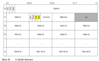
TCAN4x5x_MRAM_Config MRAMConfiguration = {
.SIDNumElements = 2, // Standard ID number of elements, you MUST have a filter written to MRAM for each element defined
.XIDNumElements = 1, // Extended ID number of elements, you MUST have a filter written to MRAM for each element defined
.Rx0NumElements = 2, // RX0 Number of elements
.Rx0ElementSize = MRAM_8_Byte_Data, // RX0 data payload size
.Rx1NumElements = 64, // RX1 number of elements
.Rx1ElementSize = MRAM_8_Byte_Data, // RX1 data payload size
.RxBufNumElements = 0, // RX buffer number of elements
.RxBufElementSize = MRAM_8_Byte_Data, // RX buffer data payload size
.TxEventFIFONumElements = 0, // TX Event FIFO number of elements
.TxBufferNumElements = 2, // TX buffer number of elements
.TxBufferElementSize = MRAM_8_Byte_Data // TX buffer data payload size
};
/* Configure the MCAN core with the settings above, the changes in this block are write protected registers, *
* so it makes the most sense to do them all at once, so we only unlock and lock once */
TCAN4x5x_MCAN_EnableProtectedRegisters(); // Start by making protected registers accessible
TCAN4x5x_MCAN_ConfigureCCCRRegister(&cccrConfig); // Enable FD mode and Bit rate switching
TCAN4x5x_MCAN_ConfigureGlobalFilter(&gfc); // Configure the global filter configuration (Default CAN message behavior)
TCAN4x5x_MCAN_ConfigureNominalTiming_Simple(&TCANNomTiming);// Setup nominal/arbitration bit timing
TCAN4x5x_MCAN_ConfigureDataTiming_Simple(&TCANDataTiming); // Setup CAN FD timing
TCAN4x5x_MRAM_Clear(); // Clear all of MRAM (Writes 0's to all of it)
TCAN4x5x_MRAM_Configure(&MRAMConfiguration); // Set up the applicable registers related to MRAM configuration
TCAN4x5x_MCAN_DisableProtectedRegisters(); // Disable protected write and take device out of INIT mode
/* Set the interrupts we want to enable for MCAN */
TCAN4x5x_MCAN_Interrupt_Enable mcan_ie = {
mcan_ie.RF0NE = 1, // RX FIFO 0 new message interrupt enable
};
TCAN4x5x_MCAN_ConfigureInterruptEnable(&mcan_ie); // Enable the appropriate registers
extern const uint16_t SET_BALANCE_VOLTAGE_BASE;
// Send Balancing Setpoint Frames From Watchdog to FIFO #0
TCAN4x5x_MCAN_SID_Filter SID_ID = {
.SFT = TCAN4x5x_SID_SFT_CLASSIC,
.SFEC = TCAN4x5x_SID_SFEC_PRIORITYSTORERX0,
.SFID1 = SET_BALANCE_VOLTAGE_BASE, // SFID1
.SFID2 = SET_BALANCE_VOLTAGE_BASE // SFID2
};
TCAN4x5x_MCAN_WriteSIDFilter(0, &SID_ID); // Write to the MRAM
// Send std frames to FIFO #1. This is dynamically set by
SID_ID.SFT = TCAN4x5x_SID_SFT_RANGE;
SID_ID.SFEC = TCAN4x5x_SID_SFEC_PRIORITYSTORERX1;
SID_ID.SFID1 = 0x200; // SFID1
SID_ID.SFID2 = 0x20F; // SFID2
TCAN4x5x_MCAN_WriteSIDFilter(1, &SID_ID); // Write to the MRAM
/* Store ID 0x12345678 as a priority message */
TCAN4x5x_MCAN_XID_Filter XID_ID = {
.EFT = TCAN4x5x_XID_EFT_RANGENOMASK, // Don't filter (id values are Don't cares)
.EFEC = TCAN4x5x_XID_EFEC_REJECTMATCH, // Ignore
.EFID1 = 0x12345678, // EFID1 (Classic mode filter)
.EFID2 = 0x1FFFFFFF // EFID2 (Classic mode mask)
};
TCAN4x5x_MCAN_WriteXIDFilter(0, &XID_ID); // Write to the MRAM
/* Configure the TCAN4550 Non-CAN-related functions */
TCAN4x5x_DEV_CONFIG devConfig = {
.SWE_DIS = 0, // Keep Sleep Wake Error Enabled (it's a disable bit, not an enable)
.DEVICE_RESET = 0, // Not requesting a software reset
.WD_EN = 0, // Watchdog disabled
.nWKRQ_CONFIG = 0, // Mirror INH function (default)
.INH_DIS = 0, // INH enabled (default)
.GPIO1_GPO_CONFIG = TCAN4x5x_DEV_CONFIG_GPO1_MCAN_INT1, // MCAN nINT 1 (default)
.FAIL_SAFE_EN = 0, // Failsafe disabled (default)
.GPIO1_CONFIG = TCAN4x5x_DEV_CONFIG_GPIO1_CONFIG_GPO, // GPIO set as GPO (Default)
.WD_ACTION = TCAN4x5x_DEV_CONFIG_WDT_ACTION_nINT, // Watchdog set an interrupt (default)
.WD_BIT_RESET = 0, // Don't reset the watchdog
.nWKRQ_VOLTAGE = 0, // Set nWKRQ to internal voltage rail (default)
.GPO2_CONFIG = TCAN4x5x_DEV_CONFIG_GPO2_NO_ACTION, // GPO2 has no behavior (default)
.CLK_REF = 1, // Input crystal is a 40 MHz crystal (default)
.WAKE_CONFIG = TCAN4x5x_DEV_CONFIG_WAKE_BOTH_EDGES // Wake pin can be triggered by either edge (default)
};
TCAN4x5x_Device_Configure(&devConfig); // Configure the device with the above configuration
TCAN4x5x_Device_SetMode(TCAN4x5x_DEVICE_MODE_NORMAL); // Set to normal mode, since configuration is done. This line turns on the transceiver
TCAN4x5x_MCAN_ClearInterruptsAll(); // Resets all MCAN interrupts (does NOT include any SPIERR interrupts)


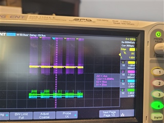
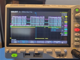
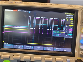
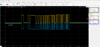
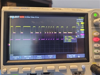
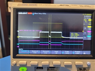 scope trace is also attached