This thread has been locked.

If you have a related question, please click the "Ask a related question" button in the top right corner. The newly created question will be automatically linked to this question.

PCA9306: I2C ACK is not coming to Zero

Part Number: PCA9306

Dear Team,

Question 1:

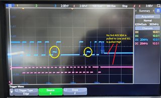
Below is the I2C wave from captured .You can see that the ACK is coming to 0.8V.May I know is this due to the presence of level shifter.

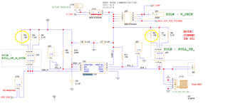
Please see my circuit below.The pull up used is 10K,LOW side voltage is 2.9V and HIGH side voltage is 5V.
Qusetion2:

You can see that two acknowledgements are coming (Yellow Circle).

After that you can see that there is no ACK and SDA pulled to LOW and SCL pulled to high.

No clock is coming after that.May I know is it an expected behaviour.I mean clock properly comes from Arduino only when it receives ACK properly.

Question 3:

Looking closely at trace(1st image), it appears that SDA is transitioning low-to-high while SCL is low. This appears to be the controller sending the STOP condition, in the middle of a frame.
Is this a firmware issue

  • The PCA9306 is a passive switch. All devices must be able to sink the total current through the pull-up resistors on both sides. Apparently, your slave device has a low drive strength. What is that slave device?

    It looks as if the master is sending the first bit of the third byte, but then sends a STOP. This does not make sense.

    The voltage of the clock signal appears to be wrong. At which points did you measure these waveforms?

  • Slave device is our company's ASIC

    The clock to the DUT is not directly given from Arduino.We are using a circuit called voltage modulator.This modulator is designed using a SPDT switch.One I/P of the switch is connected to 3.8V and another I/P is connected to 2.9V.The clock coming from Arduino is used as a control signal for this SPDT switch.If CLK is high output will be 3.8V and when it is low the output will be 2.9V.

    This 2.9V and 3.8V is coming from a Power analyzer(Key sight N6705C).The 2.9V is also connected to VREF_LOW of the level shifter. The modulator circuit is given below.

  • What is the drive strength of that ASIC?

    Please capture SDA and SCL at both the master and the DUT, and zoom in at the time after the second ACK.

  • Hari,

    Below is the I2C wave from captured .You can see that the ACK is coming to 0.8V.May I know is this due to the presence of level shifter.

    Please see my circuit below.The pull up used is 10K,LOW side voltage is 2.9V and HIGH side voltage is 5V.

    It could be possible that the target (slave) device is not able to sink the total current of both 10kohm pull-ups on both sides of the level translator (Clemens mentioned this in his response). PCA9306 is a passive device that implements a passFET internally for level translating. This means that pull-ups on both sides of the translator will appear somewhat in parallel. 10kohm || 10kohm = 5kohm pull-up. The driver of the slave (target) device must be capable of overcoming the strength of a 5kohm pull-up, not a 10kohm pull-up. 

    You can see that two acknowledgements are coming (Yellow Circle).

    After that you can see that there is no ACK and SDA pulled to LOW and SCL pulled to high.

    No clock is coming after that.May I know is it an expected behaviour.I mean clock properly comes from Arduino only when it receives ACK properly.

    This is behavior specific to Arduino, not the PCA9306. 

    I would suspect this is expected behavior of the Arduino device. Since Arduino is being used as the master (controller) device in this case, it is responsible for generating the CLK pulses on SCL. After successful ACK, the Arduino knows to write 8 cycles on the clock for each successful write/read command. If a NACK is received, there is no reason for the Arduino to continue clocking. 

    Looking closely at trace(1st image), it appears that SDA is transitioning low-to-high while SCL is low. This appears to be the controller sending the STOP condition, in the middle of a frame.
    Is this a firmware issue

    The bus master (Arduino) must first release the SCL line and SDA must transition from LOW-to-HIGH while SCL is idle for a stop condition to bet met. I am not seeing the SCL line being released in the middle of the frame.

    I think for next steps in debug we should gather more information on what is happening on the I2C bus. Please follow Clemens suggestions in gathering scope captures at both the master and slave device SDA/SCL signals all on the same scope. We need to make sure what the master device is sending is what is received at the slave device. 

    Regards,

    Tyler

  • Thank you.Definitely I wll capture and update in this forum.