This thread has been locked.

If you have a related question, please click the "Ask a related question" button in the top right corner. The newly created question will be automatically linked to this question.

THVD8000: Circuit design

Part Number: THVD8000

I have purchased THVD8000 samples through MOUSER on-line.

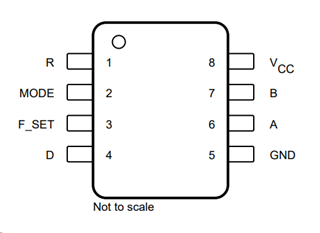
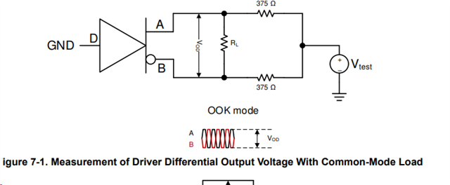
So, I tried to do the measurement by Fig.7-1 of THVD800 datasheet for checking OOK mode.

But, I could not see the waveform of OOK signal on the oscilloscope.

Please explain the method in detail and let me know the check point.

Thanks,

Greg

  • Hi Greg,

    So figure 7-1 doesn't show all necessary connections for operation - so I will run through each pin and how it should be connected to measure the OOK signal. 

    First - just as a basic understanding of how the device works; when the device is in transmit mode it will convert a logic high at the "D" input  a 0V differential signal between "A" and "B" will be driven. When there is a logic low at the "D" input a pulse train of frequency Fmod (set by end user through F_SET pin)  will be generated between "A" and "B". 

    Using the THVD8000 pinout as shown above I will run through each pin and what you need to do to measure the pulse train between "A" and "B". 

    Pin 1 "R" - This pin will be high-z when the device is in transmit mode. Depending on higher level protocol used with THVD8000 a common use case is to pull-up this pin up with a resistor so that  its default output state is "high". For testing of the driver this pin can be left floating since it would be unused in that kind of test. 

    Pin 2 "MODE" - This pin needs to be held at an input voltage of 2V up to VCC to keep the device in transmit mode. When MODE = Logic High the THVD8000 is in transmit mode - to measure the output OOK signal the device needs to be in transmit mode. For RX mode MODE = Logic Low. 

    Pin 3 "F_SET" - this pin sets the modulation frequency of the modulator for driving (and demodulator for reception). This is set by a resistor from this pin to ground. The value of which should be according to the table below. I will note that we recommend a maximum resistor tolerance of +/-2% or lower to maintain the +/-25% tolerance on modulation frequency. 


    So, for example,  if you want a 750kHz modulation frequency the F_SET resistor to ground value would be 12.5k Ohms. We recommend that the max data rate of the signal is no more than 1/10th of the modulation frequency and the power coupling network passive value do decrease with an increase of modulation frequency. 

    Pin 4 "D" - This is your input pin for the driver. It should be pulled low (to GND) to send a pulse train out between "A" and "B" pins in transmit mode. 

    Pin 5 "GND" - Ground this pin. 

    Pin 6 and Pin 7 "A" and "B" -  for this specific test you can follow figure 7-1 as shown for "A", "B", and "D" :

    VTEST is generally going to be from -7V to 12V to help model a ground potential difference. 

    Pin 8 "VCC" - connect this pin to a 3V to 5.5V source (5V operation is going have best performance) and have a 100nF capacitor to GND near the VCC pin for IC decoupling. 

    So in conclusion:

    "R" pin - can be left floating for driver test

    "MODE" pin - connect to VCC for TX mode. 

    "F_SET" pin - place resistor to ground from pin with value based on Table 8-1 linked in this post + datasheet (pages 14-15)

    "D" pin - Ground this pin to generate an OOK pulse train between "A" and "B". Pulling this pin high will create 0V between A and B. 

    "GND" pin - Ground this pin.

    "A" and "B" pins - follow figure 7.1

    "VCC" pin  - connect to 3V to 5.5V supply with a 100nF capacitor to GND near VCC for supply decoupling. 

    Please let me know if you have any other issues or if you have any additional questions and I will see what I can do!

    Best,

    Parker Dodson

  • Thanks, Parker.

    I am sorry that the reason is why there was a micro cold-soldering.

    But your answer was very helpful for me.

    Best regards,

    Greg