This thread has been locked.

If you have a related question, please click the "Ask a related question" button in the top right corner. The newly created question will be automatically linked to this question.

DP83867IR: Regarding the PCB LAYOUT problem of the RGMII interface of DP83867IR

Part Number: DP83867IR

HI,Team

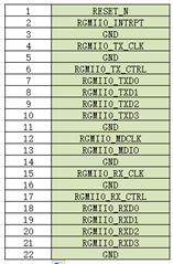
Regarding the RGMII signals of DP83867IRRGZT, they include TX_CLK, TX_D[3:0], RX_CLK, RX_D[3:0], TX_CTRL, RX_CTRL, MDC, MDIO, INT_PWDN, RESET_N. What are the signal spacing requirements in PCB LAYOUT? If grouped according to read and write, MDC, MDIO, INT_PWDN, RESET_N, can they be assigned to the read group or write group? Or a separate group?Thank you so much.

  • Hi Sheng,

    The general rule of thumb is that all single ended signals need to be routed for 50 Ohm characteristic impedance, with RGMII typically being up to 6" long at most, but recommended under 2". Spacing recommendation is not set in stone, but a good rule of thumb is that the RGMII traces should be 5 * (Trace width) away from each other. For Reset/MDC/MDIO/PWDN, there is no guidelines as these are lower frequency signals.

    Sincerely,

    Gerome

  • Hi Gerome.

    thank you for your reply.

    As shown in the figure below, the signal is planned to go to a connector, and the pin pitch of the connector is 0.5mm. Since there are not enough pins, I want to delete some of the GND pins. I think it is still necessary to retain the GND pin on both sides of the clock signal. Can the GND of pin 11 in the picture be removed? Does the GND pin need to be isolated between read and write signals? Do you have any good opinions? Can you help me optimize this signal arrangement? The 5W line spacing is good but difficult to achieve. Thanks.

  • Hi Sheng,

    I am unsure of the ask here. It appears that all of the necessary RGMII traces are present on this connector. I do not have an answer to your question of GND being needed to isolate between read and write signals as in general, if the signals are going through a connector, the spacing can't be obeyed as the signals are routed in such a small area; therefore it is inherently an imperfection on the signal chain. 

    Sincerely,

    Gerome

  • Hi Gerome.

    thank you for your reply.

    Because the pin spacing of the connector is 0.5mm, I think it can meet the line width spacing of 3W. If it is a clock signal pin, it is necessary to add GND pins on both sides. If it is other signals, is there no need to add GND? Signal? Is it okay to just use the pin spacing to meet 3W?

  • Hi Sheng,

    We do not have recommendation on this type of topic unfortunately. As mentioned prior, as all the signals will need to be squeezed through the connector, there is no avoiding violating the spacing constraint; only to have this guidance be present on a majority of the traces away from connector.

    Sincerely,

    Gerome