This thread has been locked.

If you have a related question, please click the "Ask a related question" button in the top right corner. The newly created question will be automatically linked to this question.

SN65DSI85-Q1: SN65DSI85-Q1 input/output limitation

Part Number: SN65DSI85-Q1
Other Parts Discussed in Thread: SN65DSI85

Hi,

I would like you to confirm whether following usecase can be acceptable or not.

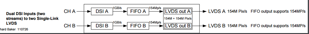
* Two input at 1920x720@60 and two output.

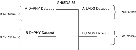
According to datasheet, it seems that up to 154MHz is limitation in case of Dual link.

So above usecase can be acceptable.

However, I would like you to confirm that my understanding is correct just in case.

So could you confirm whether my understanding is correct or not ?

Best Regards,

Machida

  • The DSI85 supports 154MHz per output channel. 

    Regards

  • Hi Joel-san,

    Sorry for my late reply.

    I have additional question.

    You said that user can input dual channel and output dual channel.

    However, according to datasheet, it seems that only one system is provided to reference clock of LVDS.

    Does it mean user can input dual DSI data and output dual LVDS data respectively, however these source and distination data should be same as limitation ?

    (Ex :

    Case 1 : Input "A_DSI : 1920x720@60 and B_DSI 1920x720@60", output "A_LVDS : 1920x720@60 and B_LVDS 1920x720@60"

    Case 2 : Input "A_DSI : 1920x720@60 and B_DSI 1280x720@60", output "A_LVDS : 1920x720@60 and B_LVDS 1280x720@60"

    Case 1 is available but case 2 is NOT available)

    I want you to confirm whether user can operate channel A and channel B separately or not.

    Best Regards,

    Machida

  • Hi Machida,

    Your understanding is correct. The output LVDS clock of both channels is derived from either the DSI channel A clock, or from an external reference clock source. Therefore, only case 1 above is suitable.

    Regards,

    Joel

  • Hi Joel-san,

    Thank you for your reply.

    Let me comfirm addtional question for your answer.

    * When user input only DSI ch B (there is no data/clock input for DSI ch A), can user output LVDS ch B ?

    In this case, user only use LVDS clock source from external reference clock (Add 0x0A[0] = 0), but I believe that there is no other limitation.

    Is my understanding correct ?

    Best Regards,

    Machida

  • Hi Machida,

    When the source for the output clock is the REFCLK, it is not necessary to have a input clock in the DSI Channel A, therefore, they can transmit only from DSI ChB to the LVDS ChB.

    Regards

  • Hi Joel-san,

    Thank you for your reply.

    >When the source for the output clock is the REFCLK, it is not necessary to have a input clock in the DSI Channel A, therefore, they can transmit only from DSI ChB to the LVDS ChB.

    In this case, it is better to use same oscillator for DSI clock source and REFCLK source, right ?
    (If different oscillator is used for DSI clock source and REFCLK source, then i think user should use line buffer of SN65DSI85 to meet timing..)

    BR,
    Machida
  • Hi Machida-san,

    Even when you use a REFCLK as source for the LVDS clock you still need a compliant DPHY DSI Clock for the Channel B. You cannot use the same clock for the DSI and REFCLK.

    Regards