


Hello,
I need a clarification about the input driving of the UCC5310M.
On paragraph 10.3.2 of datasheet I can read: "If any of the inputs are left open, 128 kΩ of internal pulldown resistance forces the IN+ pin low and 128 kΩ of internal resistance pulls IN– high. However, TI still recommends grounding an input or tying to VCC1 if it is not being used for improved noise immunity."
Accordingly to such sentence, the application example in paragraph 11.2 is:
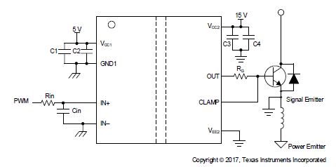
Where I expect OUT goes to high when PWM signal goes to high.
But the functional table in paragraph 10.4 is:

With internall pull-up and pull-down resistors IN+ is normally tied to low and IN- is normally tied to high, so in the application schema above it seems impossible for the OUT to goes high.
Is that correct or am I misunderstanding anything?
Thank you in advance for any clarification
Best regards
Matteo

