This thread has been locked.

If you have a related question, please click the "Ask a related question" button in the top right corner. The newly created question will be automatically linked to this question.

TUSB1210: Host and Device operation for TUSB1210 (EVM)

Part Number: TUSB1210

For my design, implementing both Case 1 and Case 3. For Case 1, using a TUSB1210 PHY to interface between a PC Host and a FPGA via the PHY ULPI pins, and for Case 3 I use another TUSB1210 PHY to interface between an FPGA and an external USB Hub. 

This is my understanding of the TUSB1210EVM:

Power Input:

+5V to CN1.2 and CN1.4

+1.8V to CN1.19 and CN1.20

All cases assume High Speed mode.

Case 1: If I want my TUSB1210 to interface to a PC USB port (the USB Host), my TUSB1210 has to be setup as a Device, data sheet page 53.

Case 2: If I want my TUSB1210 to interface to a USB Device (a peripheral such as a mouse or keyboard), my TUSB1210 has to be setup as a Host, data sheet page 48.

Case 3: What if I want to interface to a USB Hub, does the Hub act as a USB "Host", therefore, the TUSB1210 has to be setup as a Device????

For Case 1, if my assumptions above are correct, 

J3 jumper I see as not being used, therefore, not populated.

J5 jumper set for 1-3 and 2-4. I do not see what J5: 1-3 does, I think it is not required.

J6 jumper set for 1-2, Output Mode for clock, use onboard 26MHz oscillator for REFCLK input.

J7 jumper is unpopulated.

J8 jumper is unpopulated, not sure what purpose this serves.

J9 jumper set for 2-3, so chip is enabled by +1.8V. I could set for 1-2 so chip is powered down when no USB cable attached.

J11 jumper is unpopulated

When I connect the USB cable from my PC USB Host to my TUSB1210 PHY acting as a Device, and apply +5V and +1.8V to CN1, my power supplies indicate +5V @ 0.04A and +1.8V @ 0.15A.

I did not expect the +1.8V to draw 150mA, since data sheet says that operating at HS Operation, should only draw a total of 48mA between VBAT, VDDIO and VDD18, data sheet page 7. Why so much current draw????

U5.20 VDD33 reads +3.3V == U5.21 VBAT, OK

U5.12 VDD15 reads +1.5V, OK

U5.17 CPEN is LOW, OK since do not want U2 to generate +5V.

U5.22 VBUS reads +5V, OK

U5.1 REFCLK has 26MHZ clock

U5.26 CLOCK has 60MHz output clock, OK

If I implement Case 2 above, I will change the following jumpers from above:

J3  jumper set for 2-3 to pass U2.5 +5V to USB cable VBUS pin

J5 jumper set for 1-2 and 3-4. 

Does J8 jumper have to be populated OR do I need to GND it through a <1k ohm resistor????

What makes the U5.17 CPEN signal go HIGH for Host mode????

I appreciate any comments.

Thanks, Roland

  • Roland

    Please see my input

    Power Input:

    +5V to CN1.2 and CN1.4 Correct
    +1.8V to CN1.19 and CN1.20 Correct
    All cases assume High Speed mode.

    Case 1: If I want my TUSB1210 to interface to a PC USB port (the USB Host), my TUSB1210 has to be setup as a Device, data sheet page 53. Correct
    Case 2: If I want my TUSB1210 to interface to a USB Device (a peripheral such as a mouse or keyboard), my TUSB1210 has to be setup as a Host, data sheet page 48. Correct
    Case 3: What if I want to interface to a USB Hub, does the Hub act as a USB "Host", therefore, the TUSB1210 has to be setup as a Device???? No, when facing TUSB1210, hub will act as a device on its upstream port.

    For Case 1, if my assumptions above are correct,

    J3 jumper I see as not being used, therefore, not populated. Correct

    J5 jumper set for 1-3 and 2-4. I do not see what J5: 1-3 does, I think it is not required. Ok

    J6 jumper set for 1-2, Output Mode for clock, use onboard 26MHz oscillator for REFCLK input. Correct

    J7 jumper is unpopulated. Correct

    J8 jumper is unpopulated, not sure what purpose this serves. Correct

    J9 jumper set for 2-3, so chip is enabled by +1.8V. I could set for 1-2 so chip is powered down when no USB cable attached. Correct

    J11 jumper is unpopulated Correct

    When I connect the USB cable from my PC USB Host to my TUSB1210 PHY acting as a Device, and apply +5V and +1.8V to CN1, my power supplies indicate +5V @ 0.04A and +1.8V @ 0.15A.

    I did not expect the +1.8V to draw 150mA, since data sheet says that operating at HS Operation, should only draw a total of 48mA between VBAT, VDDIO and VDD18, data sheet page 7. Why so much current draw???? Need further debug, do you have a controller connected to TUSB1210?

    U5.20 VDD33 reads +3.3V == U5.21 VBAT, OK

    U5.12 VDD15 reads +1.5V, OK

    U5.17 CPEN is LOW, OK since do not want U2 to generate +5V.

    U5.22 VBUS reads +5V, OK

    U5.1 REFCLK has 26MHZ clock

    U5.26 CLOCK has 60MHz output clock, OK

    If I implement Case 2 above, I will change the following jumpers from above:

    J3 jumper set for 2-3 to pass U2.5 +5V to USB cable VBUS pin Correct

    J5 jumper set for 1-2 and 3-4. Correct

    Does J8 jumper have to be populated OR do I need to GND it through a <1k ohm resistor????

    ID pin connects to GND for USB host and floating for USB device. 

    What makes the U5.17 CPEN signal go HIGH for Host mode???? Both DRVVBUS and DRVVBUSEXTERNAL bits must be set to 1 in order to to set Pin17 (CPEN).

    Thanks

    David

  • David,

    Thank you for the response.

    This thread is a "continuation" and has more details than my other thread:

    TUSB1210: Implement KVM over fiber with TUSB1210

    https://e2e.ti.com/support/interface/f/138/t/755953

    FROM PREVIOUS RESPONSE:

    "Case 1: If I want my TUSB1210 to interface to a PC USB port (the USB Host), my TUSB1210 has to be setup as a Device, data sheet page 53. Correct

    Case 2: If I want my TUSB1210 to interface to a USB Device (a peripheral such as a mouse or keyboard), my TUSB1210 has to be setup as a Host, data sheet page 48. Correct

    Case 3: What if I want to interface to a USB Hub, does the Hub act as a USB "Host", therefore, the TUSB1210 has to be setup as a Device????

    David response: No, when facing TUSB1210, hub will act as a device on its upstream port."

    OK, so for Case 3 above, it acts like Case 2.

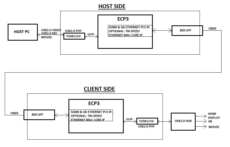
    Therefore, summarizing from the block diagram in my other case mentioned, Case 1 is implemented on the HOST SIDE and Case 2 is implemented on the CLIENT SIDE.Including block diagram again, see below.

    No ETHERNET MAC CORE IP will be used in the FPGA's.

    FROM PREVIOUS RESPONSE:

    For Case 1 description above: " Why so much current draw????

    David response: Need further debug, do you have a controller connected to TUSB1210?"

    RF response:       There is no USB device controller connected to the ULPI interface. We are planning on  transferring the ULPI data from the HOST SIDE ECP3 FPGA to the CLIENT SIDE ECP3 FPGA ULPI interface ( a "transparent" link).

    There will be no USB device controller on the HOST SIDE ECP3 and no Host controller on the CLIENT SIDE ECP3.

    We are hoping that this scheme will work.

    Thanks, Roland

  • David,
    Also, the TI TUSB1210 EVM SLLU208 pdf is missing the bottom third of Fig 2 Power Supply. It is in the OrCAD schematic
    Thanks, Roland
  • Roland

    Yes, thanks for point it out, the user guide needs to be updated to fix this mistake.

    Going back to your question, TUSB1210 is a transceiver (PHY) only, the definition and functionality of being host or device lies with the link controller. Without a link controller, TUSB1210 does not exist as a host or a device, it is simply a PHY. Request generated by host will not be responded by the TUSB1210, TUSB1210 will only pass the data from USB to ULPI, and from ULPI to USB, the hub will respond to host request. And this goes back to what we discussed before, that the hub response time will potentially be an issue depending on the total system propagation delay.

    On the power consumption question, I attached a copy of ULPI spec: www.sparkfun.com/.../ULPI_v1_1.pdf. Section 3.8.5 focuses on USB operation. USB operation depends on the state of TUSB1210 ULPI interface, which is driven by the FPGA. So we first need to look at the state of each ULPI control pins in order to know the state of TUSB1210.

    Thanks
    David
  • David,
    Since I will not have a 5-pin USB cable (no ID pin), is the following correct:
    TUSB1210 setup as a Device, I will have U5.23 ID pin floating
    TUSB1210 setup as a Host, I will have U5.23 ID pin directly connected to GND

    Thanks, Roland
  • Roland

    Correct, the ID pin is typically set by the cable itself, but you can force it as you described in your response.

    Thanks
    David
  • David,
    Does the VBUS pin draw any current. No mention in data sheet.
    Thanks, Roland
  • Roland

    VBUS is used as a sensing pin as part of the USB OTG implementation, we do not use VBUS to power any internal circuit, so the power on VBUS is very minimal.

    Thanks
    David
  • David,
    If I want to tie RESETB to VDDIO (1.8V) if RESETB is unused, is there an internal pull down on the RESETB input? If not, I should supply a 100k ohm pull down.
    Thanks, Roland
  • Roland

    I would tie RESETB to VDDIO through a 10k resistor, but you do not need 100k pulldown.

    Thanks
    David
  • David,

    The TUSB1210 EVM has series 22 ohm resistors on the Data, 60 MHz CLOCK output, STP, DIR and NXT signals.

    My TUSB1210 interfaces to a Lattice ECP3 FPGA, distance between them probably will be at most 1.5".

    For my design I specified series 0201 size 22 ohm resistors.

    Do I require the series 22 ohm resistors?

    How critical is the physical size of the series resistors, if they are required? EVM uses 0402 size 22 ohm resistors.

    I would like to specify 0402 size resistors, since they are easier to do rework on if I need to find an optimal value. Project is in rush mode.

    If series resistors are required:

    - do I place closer to TUSB1210 outputs or ECP3 FPGA inputs?

    - how do I determine optimal value?

    I specified the Zo, characteristic impedance, as 50 ohms for these signals. Is this correct?

    Thanks, Roland

  • Roland

    This comes from having both full speed and high speed in the same system. When using a full speed (12Mbps) buffer in a USB 2.0 system, it is necessary to place a series resistor on the D+ and D− pins external to the transceiver. This placement is a result of the need to properly match the impedance of the specified transmission line having a differential characteristic impedance (ZO) of 90Ω and a single ended impedance of 45Ω. To match this load, it requires that the full speed transceiver output impedance must be in the range 28Ω to 44Ω. Section 7.1.1.1 of the USB2.0 spec has further detail on it.

    Size 402 is fine, and the placement of the series resistor is less critical in this case.

    Thanks
    David
  • David,

    I am referring to the series 22 ohm resistors on Data[0..7], 60 MHz CLOCK output, STP, DIR and NXT signals.
    The EVM does not have any series resistors on the D+ or D- USB signals.
    I did not see any input impedance or output impedance spec on the non-USB signals in the data sheet.
    Specifying Zo characteristic impedance of 50 ohms for my Data[0..7], 60 MHz CLOCK output, STP, DIR and NXT single-ended signals.
    I am including 0402 size 22 ohm series resistors, similar to EVM, unless you tell me they are not required. I figure I can always short the 22 ohm resistors if not needed.
    Thanks, Roland
  • Roland

    For Data[0..7], 60 MHz CLOCK output, STP, DIR and NXT signal, the impedance is 50ohms.

    The 22ohm resistor is used as edge rate control, I would leave them as a placeholder, and can be tuned, if needed, to met TUSB1210 input timing requirement.

    Thanks
    David
  • David,
    Thank you, Roland