This thread has been locked.

If you have a related question, please click the "Ask a related question" button in the top right corner. The newly created question will be automatically linked to this question.

SN75176A: High fallout "bug"?

Part Number: SN75176A
Other Parts Discussed in Thread: THVD1500

Hello,  We use the device in one of our products for RS-485 communications.  In our last couple builds, we are seeing a very high fallout in our final testing. about 5%.

We had simply asked our contract manufacturer to replace the chip and we would sort it out later.  Today I tested a bunch of boards pulled from final test, and the SN75176A devices are failing with a very odd bug, seems to be logic related.  The devices transmit data just fine.  But once we finish sending a byte of data and toggle the RE and DE pins low together to enable receive, about 70 microseconds later, the R pin on the SN75176A toggles high on its own without any change on the RS-485 bus.  Once the RS-485 bus goes low, it seems to "reset" the buggy logic in the device and the rest of the changes in the bus are translated properly.

Is this a known issue?  Is TI making steps to correct this?

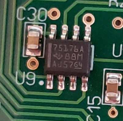
Photo of example parts:

  • Hi Jeff,

    Could you please show us a schematic of your usage of this device?  I'm mostly curious what is on the RS-485 signal lines as well as the R output pin.

    Could you please show us waveform captures showing the behavior you describe?  This isn't an issue I've heard of so I'd like to make sure we understand it.  Most of the time the "R" output would be high after toggling into receive mode since the last bit transmitted is typically a high-level "stop" bit - is this not the case in your application?  And, is the expected idle state of the bus a logic low or high state?  Is there any biasing circuitry that sets a differential offset voltage on the bus when all the drivers are disabled, or does the differential voltage drop to ~0 V in this case?

    Regards,
    Max

  • Hello Max,

    Thanks for the reply.  I did a more in-depth log with a logic analyzer, and now I understand what is happening, but don't think the behavior of the device is proper.

    I have attached two jpegs, one of the schematic snippet of the 485 transceiver, the other the logic waveforms.  The circuit is really simple, RO and DI are connected to optoisolators to feed our controller.  We have nothing on the bus A and B lines, so my board tester simply has another one of our boards to act as a slave.  Our board is basically a smart protocol converter, so we ping between the DUT and the slave board for all the various protocols.

    At idle, we rely on a HI state for the 485 line, and since all of our protocols except CAN are bit-banged, to read bytes we rely on interrupts, so for the 485 we look for a falling edge.

    See the attached waveforms.  Line 2 (RED) is where the device under test sends out a byte of data (0xA6).  Since this is a closed system, instead of using my mixed analog and digital analyzer, I simply used the digital log on the actual bus lines.  (wont show the actual voltages, but know whether the voltage on the bus is above logic level or not)

    You can see that the proper signal is on the BUS A and B, then Line 3 (Orange) shows the byte of data at the RO pin of the Slave board.

    Everything so far is OK!

    However, shortly after sending out the byte, I toggle the RE\ DE lines low (Line 0, White trace) , to switch the Master device from transmit mode to receive mode.  At this point, both the Master and the Slave devices are in Receive mode, so the bus is effectively floating.  I don't know the exact voltages present on the bus A and B, but you can see that somehow the BUS B line is getting pulled high, consequently the Master RO line is getting pulled Low.  

    My current slave software enables the Drive line right before the slave starts transmitting the response byte.  However, it is too late to catch the start bit of the byte, so my interrupt on the Master doesn't see the start bit.  

    I was able to easily "fix" the tester by simply changing the slave software to toggle the RE\ DE line high immediately after it reads the byte from the master. 

    HOWEVER, in our application, we don't talk to another one of our boards, we talk to a number of other single-ended controllers where I have no idea what idle state their 485 controller is on the bus.  It might be biased high, but might not be.  Furthermore, I believe the device as shown is not matching the specs on the TI datasheet.  The datasheet logic chart shows that with open bus and RE\ DE pulled low, then RO should be High.  That is not what is happening here.  So although I can "fix" my tester to pass these devices, but I don't know if I am risking field problems by putting these out in the field.  (All the units exhibiting this behavior haven't made it out to the field; we have been swapping out the 485 transceivers when this happens on the test stand)

    Your thoughts are appreciated.

    Jeff

  • Had to open another reply to attach the waveforms

  • Had to open another reply to attach the waveforms

  • Hi Jeff,

    Thanks for the waveforms and further description!  This really helps clear things up.

    Where are you seeing that the receiver output should be high when /RE is low and the bus input is left open?  Per the Receiver Function Table (Table 3 on page 12 of the SN75176A datasheet, link here: http://www.ti.com/lit/ds/symlink/sn75176a.pdf) it looks like the receiver output is undefined when there is an open-input condition.  This is because this condition typically results in a differential input voltage close to 0 V, which is not large enough to be reliably interpreted as "high" (which requires >200 mV per "VIT+" spec) and not low enough to be reliably interpreted as "low" (which requires <200 mV per "VIT-" spec).  It sounds like when you are using some units whose input threshold is biased towards the more negative direction your system works (since 0 V is then interpreted as high), but when you are using units whose input threshold is biased towards the more positive direction your system does not work (since 0 V is then interpreted as low).

    If your system relies on all nodes reporting a "high" level when no transmitter circuits are active (as many RS-485 implementations do), then you would either need to implement a bias externally via pull-up resistance on A and pull-down resistance on B or migrate to another transceiver that has what is called internal "failsafe" biasing.  This usually looks like VIT+/VIT- thresholds that are both negative, allowing for a 0-V input to always be considered high.

    To read more about internal failsafe biasing, you could refer to this blog:

    https://e2e.ti.com/blogs_/b/analogwire/archive/2016/02/09/rs-485-basics-the-rs-485-receiver

    To read more about external failsafe biasing, you could refer to this blog:

    https://e2e.ti.com/blogs_/b/industrial_strength/archive/2016/12/06/rs-485-basics-two-ways-to-fail-safe-bias-your-network

    An example of a pin-for-pin update to SN75176A with internal failsafe biasing is THVD1500.

    Please let me know if any of this info is unclear or if you think I am overlooking something.

    Regards,
    Max