This thread has been locked.

If you have a related question, please click the "Ask a related question" button in the top right corner. The newly created question will be automatically linked to this question.

CCS/TCAN4550-Q1: TCAN4550 SPI Communication problem with TMS320F280040 (C2000).

Part Number: TCAN4550-Q1
Other Parts Discussed in Thread: TCAN4550, BOOSTXL-CANFD-LIN

Tool/software: Code Composer Studio

Hello~!.

I’m Alex.Kim, And I’m in problem with TCAN4550-Q1.

Now, I’m developing product using TCAN4550 for CAN-FD.

And, I have made TCAN4550 SPI Drv. But I think It’s not working now.

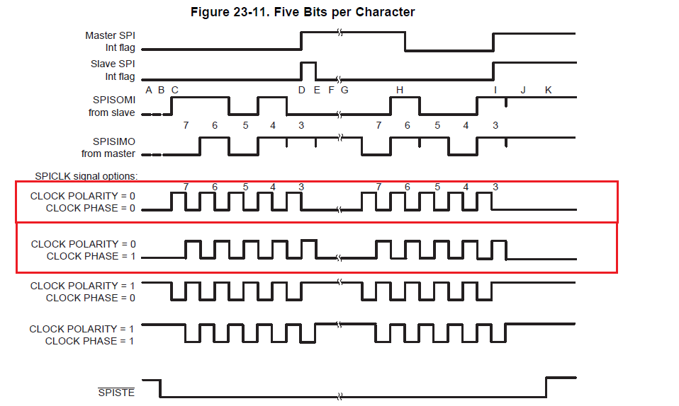
I referred datasheet came from TI like below while developing a SPI Drv.

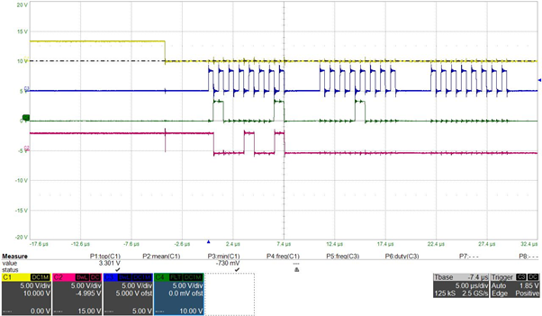
As a result, I’ve made result like below. (Read mode register(0x800) frequently.)

Yellow: nCS, Blue: SCK, Green: SDO (based on MCU), Red: SDI (based on MCU)

At the first time, I thought, It worked very well.

But all of sudden I realized that there were some troubles like below.

First problem is that sometime I can’t read correct data came from TCAN4550 through SDI.


Second problem is that some minute later MCU can’t any data unless TCAN4550 IC gets H/W reset. I mean, I just can read 0xFFFFFFFF like below picture before 


I have made driver by referring to example code “Code_sllc469a”. And My SPI Driver consist of 8bit communication. To be honest I can’t understand why SPI communication failed. So that’s why I need help by you guys. 

Please, If you have any opinion which can solve it. Don't hesitate notice me.

--- source code --

#1. TCAN4x5x_SPI.c code

/*
* TCAN4x5x_SPI.c
* Description: This file is responsible for abstracting the lower-level microcontroller SPI read and write functions
*
*
*
* Copyright (c) 2019 Texas Instruments Incorporated. All rights reserved.
* Software License Agreement
*
* Redistribution and use in source and binary forms, with or without
* modification, are permitted provided that the following conditions
* are met:
*
* Redistributions of source code must retain the above copyright
* notice, this list of conditions and the following disclaimer.
*
* Redistributions in binary form must reproduce the above copyright
* notice, this list of conditions and the following disclaimer in the
* documentation and/or other materials provided with the
* distribution.
*
* Neither the name of Texas Instruments Incorporated nor the names of
* its contributors may be used to endorse or promote products derived
* from this software without specific prior written permission.
*
* THIS SOFTWARE IS PROVIDED BY THE COPYRIGHT HOLDERS AND CONTRIBUTORS
* "AS IS" AND ANY EXPRESS OR IMPLIED WARRANTIES, INCLUDING, BUT NOT
* LIMITED TO, THE IMPLIED WARRANTIES OF MERCHANTABILITY AND FITNESS FOR
* A PARTICULAR PURPOSE ARE DISCLAIMED. IN NO EVENT SHALL THE COPYRIGHT
* OWNER OR CONTRIBUTORS BE LIABLE FOR ANY DIRECT, INDIRECT, INCIDENTAL,
* SPECIAL, EXEMPLARY, OR CONSEQUENTIAL DAMAGES (INCLUDING, BUT NOT
* LIMITED TO, PROCUREMENT OF SUBSTITUTE GOODS OR SERVICES; LOSS OF USE,
* DATA, OR PROFITS; OR BUSINESS INTERRUPTION) HOWEVER CAUSED AND ON ANY
* THEORY OF LIABILITY, WHETHER IN CONTRACT, STRICT LIABILITY, OR TORT
* (INCLUDING NEGLIGENCE OR OTHERWISE) ARISING IN ANY WAY OUT OF THE USE
* OF THIS SOFTWARE, EVEN IF ADVISED OF THE POSSIBILITY OF SUCH DAMAGE.
*/


#include "TCAN4x5x_SPI.h"
#include "Spi_Driver.h"

/*
* @brief Single word write
*
* @param address A 16-bit address of the destination register
* @param data A 32-bit word of data to write to the destination register
*/
void
AHB_WRITE_32(uint16_t address, uint32_t data)
{
AHB_WRITE_BURST_START(address, 1);
AHB_WRITE_BURST_WRITE(data);
AHB_WRITE_BURST_END();
}


/*
* @brief Single word read
*
* @param address A 16-bit address of the source register
*
* @return Returns 32-bit word of data from source register
*/
uint32_t
AHB_READ_32(uint16_t address)
{
uint32_t returnData;

AHB_READ_BURST_START(address, 1);
returnData = AHB_READ_BURST_READ();
AHB_READ_BURST_END();

return returnData;
}


/*
* @brief Burst write start
*
* The SPI transaction contains 3 parts: the header (start), the payload, and the end of data (end)
* This function is the start, where the register address and number of words are transmitted
*
* @param address A 16-bit address of the destination register
* @param words The number of 4-byte words that will be transferred. 0 = 256 words
*/
void
AHB_WRITE_BURST_START(uint16_t address, uint8_t words)
{
//set the CS low to start the transaction
Spi_ManualCsOn_8Bit(SpiObjectConfigId_TCAN4550);

Spi_TransmitData_8Bit(SpiObjectConfigId_TCAN4550, AHB_WRITE_OPCODE);

// Send the 16-bit address
Spi_TransmitData_8Bit(SpiObjectConfigId_TCAN4550, (uint8_t)((address >> 8) & 0x00FF));
Spi_TransmitData_8Bit(SpiObjectConfigId_TCAN4550, (uint8_t)((address >> 0) & 0x00FF));

// Send the number of words to read
Spi_TransmitData_8Bit(SpiObjectConfigId_TCAN4550, (uint8_t)((uint16_t)words & 0x00FF));
}


/*
* @brief Burst write
*
* The SPI transaction contains 3 parts: the header (start), the payload, and the end of data (end)
* This function writes a single word at a time
*
* @param data A 32-bit word of data to write to the destination register
*/
void
AHB_WRITE_BURST_WRITE(uint32_t data)
{
Spi_TransmitData_8Bit(SpiObjectConfigId_TCAN4550, (uint8_t)((data >> 24) & 0x000000FF));
Spi_TransmitData_8Bit(SpiObjectConfigId_TCAN4550, (uint8_t)((data >> 16) & 0x000000FF));
Spi_TransmitData_8Bit(SpiObjectConfigId_TCAN4550, (uint8_t)((data >> 8) & 0x000000FF));
Spi_TransmitData_8Bit(SpiObjectConfigId_TCAN4550, (uint8_t)((data >> 0) & 0x000000FF));
}


/*
* @brief Burst write end
*
* The SPI transaction contains 3 parts: the header (start), the payload, and the end of data (end)
* This function ends the burst transaction by pulling nCS high
*/
void
AHB_WRITE_BURST_END(void)
{
Spi_ManualCsOff_8Bit(SpiObjectConfigId_TCAN4550);
}


/*
* @brief Burst read start
*
* The SPI transaction contains 3 parts: the header (start), the payload, and the end of data (end)
* This function is the start, where the register address and number of words are transmitted
*
* @param address A 16-bit start address to begin the burst read
* @param words The number of 4-byte words that will be transferred. 0 = 256 words
*/
void
AHB_READ_BURST_START(uint16_t address, uint8_t words)
{
// Set the CS low to start the transaction
Spi_ManualCsOn_8Bit(SpiObjectConfigId_TCAN4550);

Spi_TransmitData_8Bit(SpiObjectConfigId_TCAN4550, AHB_READ_OPCODE);

// Send the 16-bit address
Spi_TransmitData_8Bit(SpiObjectConfigId_TCAN4550, (uint8_t)((address >> 8) & 0x00FF));
Spi_TransmitData_8Bit(SpiObjectConfigId_TCAN4550, (uint8_t)((address >> 0) & 0x00FF));

// Send the number of words to read
Spi_TransmitData_8Bit(SpiObjectConfigId_TCAN4550, (uint8_t)((uint16_t)words & 0x00FF));
}


/*
* @brief Burst read start
*
* The SPI transaction contains 3 parts: the header (start), the payload, and the end of data (end)
* This function where each word of data is read from the TCAN4x5x
*
* @return A 32-bit single data word that is read at a time
*/
uint32_t
AHB_READ_BURST_READ(void)
{
uint16_t readData;

uint8_t readData0;
uint8_t readData1;
uint8_t readData2;
uint8_t readData3;
uint32_t returnData;

Spi_ReceiveData_8Bit (SpiObjectConfigId_TCAN4550, 0x00, &readData);
readData0 = (uint8_t)readData;

Spi_ReceiveData_8Bit (SpiObjectConfigId_TCAN4550, 0x00, &readData);
readData1 = (uint8_t)readData;

Spi_ReceiveData_8Bit (SpiObjectConfigId_TCAN4550, 0x00, &readData);
readData2 = (uint8_t)readData;

Spi_ReceiveData_8Bit (SpiObjectConfigId_TCAN4550, 0x00, &readData);
readData3 = (uint8_t)readData;

returnData = (((uint32_t)readData0) << 24) | (((uint32_t)readData1 << 16)) | (((uint32_t)readData2) << 8) | readData3;

return returnData;
}


/*
* @brief Burst write end
*
* The SPI transaction contains 3 parts: the header (start), the payload, and the end of data (end)
* This function ends the burst transaction by pulling nCS high
*/
void
AHB_READ_BURST_END(void)
{
Spi_ManualCsOff_8Bit(SpiObjectConfigId_TCAN4550);
}

#2.  Test code

//execute every 10ms

void TCAN4550_Test (void)
{
    TCAN4550_AllReg.ModeOperationReg.word = AHB_READ_32(REG_DEV_MODES_AND_PINS); /* 0x0800 */

}

#3. Dev setting

devConfig.word = 0;
devConfig.SWE_DIS = 0; // Keep Sleep Wake Error Enabled (it's a disable bit, not an enable)
devConfig.DEVICE_RESET = 0; // Not requesting a software reset
devConfig.WD_EN = 0; // Watchdog disabled
devConfig.nWKRQ_CONFIG = 1; // Mirror INH function (default)
devConfig.INH_DIS = 1; // INH enabled (default)
devConfig.GPIO1_GPO_CONFIG = TCAN4x5x_DEV_CONFIG_GPO1_MCAN_INT1; // MCAN nINT 1 (default)
devConfig.FAIL_SAFE_EN = 0; // Failsafe disabled (default)
devConfig.GPIO1_CONFIG = TCAN4x5x_DEV_CONFIG_GPIO1_CONFIG_GPO; // GPIO set as GPO (Default)
devConfig.WD_ACTION = TCAN4x5x_DEV_CONFIG_WDT_ACTION_nINT; // Watchdog set an interrupt (default)
devConfig.WD_BIT_RESET = 0; // Don't reset the watchdog
devConfig.nWKRQ_VOLTAGE = 0; // Set nWKRQ to internal voltage rail (default)
devConfig.GPO2_CONFIG = TCAN4x5x_DEV_CONFIG_GPO2_NO_ACTION; // GPO2 has no behavior (default)
devConfig.CLK_REF = 1; // Input crystal is a 40 MHz crystal (default)
devConfig.WAKE_CONFIG = TCAN4x5x_DEV_CONFIG_WAKE_BOTH_EDGES;// Wake pin can be triggered by either edge (default)

  • Hello Alex,

    From your description of the problem, I think this is a simple issue for a device failsafe feature you might not be aware of or have understood correctly and the device is entering Sleep Mode after a timer is expiring after having expected one of a couple of different events occurring.  This is an easy problem to have during the early stages of development and debug because your code may not be fully functional or include the mechanisms to prevent or disable this feature.  If I am correct about the cause, it may have absolutely nothing to do with your SPI driver code.  Before we start any debug efforts on the code itself, I would like you to first eliminate this feature as an option.  If you still have issues, then we can take a closer look at the code.

    I will refer you to section 8.4.2 of the TCAN4550 datasheet which describes Standby Mode.  The last paragraph of this section states the following:

    Upon power up, a power on reset or wake event from sleep mode the TCAN4550 enters standby mode.  This starts a four minute timer, tINACTIVE, that requires the processor to either reset the interrupt flags or configure the device to normal mode.  This feature makes sure the node is in the lowest power mode if the processor does not come up properly.  This automatic mode change also takes place when the device has been put into sleep mode and receives a wake event, WUP or LWU.  To disable this feature for sleep events register 16'h0800[1] (SWE_DIS) must be set to one.  This will not disable the feature when powering up or when a power on reset takes place.

    Section 8.4.5 of the datasheet discusses this failsafe feature as well in the following way:

    The TCAN4550 has three methods the failsafe feature is used in order to reduce node power consumption for a node system issue.  Failsafe is the method the device uses to enter sleep mode from various other modes when specific issues arise.  This feature uses the Sleep Wake Error (SWE) timer to determine if the node processor can communicate to the TCAN4550.  The SWE timer is default enabled through the SWE_DIS; 16'h0800[1] = 0 but can be disabled by writing a one to this bit.  Even when the timer is disabled, a power on reset re-enables the timer and thus be active.  Failsafe Feature is default disabled but can be enabled by writing a one to 16'0800[13], FAILSAFE_EN.

    Upon power up the SWE timer starts, tINACTIVE, the processor has typically four minutes to configure the TCAN4550, clear the PWRON flag or configure the device for normal mode; see figure 32.  This feature cannot be disabled.  If the device has not had the PWRON flag cleared or been placed into normal mode, it enters sleep mode.  The device wakes up if the CAN bus provides a WUP or a local wake event takes place, thus entering standby mode.  Once in standby mode, tSILENCE and tINACTIVE timers start.  If tINACTIVE expires, the device re-enters sleep mode.

    The second failure mechanism that causes the device to use the failsafe feature, if enabled, is when the device receives a CANINT, CAN bus wake (WUP) or WAKE pin (LWU), while in sleep mode such that the device leaves sleep mode and enters standby mode.  The processor has four minutes to clear the flags and place the device into normal mode.  If this does not happen the device enters sleep mode.

    The third failure mechanism that causes the device to use the failsafe feature is when the standby or normal mode and the CANSLNT flag persists for tINACTIVE, the device enters sleep mode.  Examples of events that could create this are CLKIN or Crystal stops working, processor is no longer working and not able to exercise the SPI bus, a go-to-sleep command comes in and the processor is not able to receive it or is not able to respond.  See state diagram Figure 33.

    From your description that your code seems to work correctly and you can write and read registers, but then after a period of time you are no longer able to read registers and require a power on reset, I expect you have allowed the Failsafe timer to expire and the device has entered sleep.  I also suspect that you don't need a power on reset to recover, and you could also toggle the WAKE pin, or provide a WUP on the CAN bus to create a wake up event.  You could try this as a verification of the root cause.

    However, I would recommend that while you are in the debug stage you disable this feature (to the extent that it can be disabled) by setting SWE_DIS = 1.  Currently you have it set to '0' which will keep this feature enabled.  But this bit is a volatile register bit and will be reset every time there is a device reset or power on reset.  As a result when you power up the device, or re-initialize the device following a device reset, you will need to reset this bit to keep the feature disabled.  Otherwise this feature is always enabled by default.  Also, in addition to disabling this bit, you still have 4 minutes to configure the device to Normal mode, or clear the Power On Flag PWRON by reading the interrupt and status registers.

    In addition to disabling the SWE_DIS bit, I would recommend adding the code to immediately enter normal mode and to clear all the interrupt flags to end the tINACTIVE timer that is running following the power up or reset event.

    I know this is a long post, but I hope it has been informative by providing the relevant information in the post itself.  Let me know if you have any questions on this feature.  Otherwise, could you please try to disable this feature, or verify you have disabled this feature and ended the 4 minute timer in your code and re-evaluate your SPI driver code?  If you still have SPI issues, we can continue to look at the driver code in more detail.

    Regards,

    Jonathan

  • Dear Jonathan.

    First of all I'm really thank you for your suggestion.

    And I’ve checked like No.1.

    1. I set SWE_DIS bit as 1. Then I was able to see that second issue is fixed. As you mentioned, This was a simple issue. Thank you

    However, I’m still in problem with first issue. (sometimes data is missing.)

    I’ve started checking several register for reading and writing.

    (

       For example. I'm using REG_DEV_TEST_REGISTERS 0x0808.

     - One time write

    Write: h61, h08, h08, h01, h55, hAA, h00, h00,
    Read: h00, h00, h00, h00, h00, h00, h00, h00,

     - 80% I read

    Write: h41, h08, h08, h01, h00, h00, h00, h00,
    Read: h00, h00, h00, h00, h55, hAA, h00, h00,

     - 20% I read

    Write: h41, h08, h08, h01, h00, h00, h00, h00,
    Read: h00, h00, h00, h00, h00, h00, h00, h00,

    )

    I think, I can’t read or write register correctly. I mean, I’m not sure whether my data is right or not through SPI.

    So, first problem have still been distressing me up. Please Would you check oscilloscope data attached before. Maybe if there is some point to be fixed, Please tell me what.

    I can't understand why sometimes I read zero data from TCAN4550 even though I use correct communication method for reading or writing.

    And I'd like to show you value for SPI in MCU like below.

    I tried 2 method POL = 0, PHA = 0, and POL = 0, PHA = 1.

    But both of them is same.

    Thank you for your response again.

    Best regards.

  • Hi Alex,

    I am glad to hear that we resolved one issue.  And before we get into the other issue, the TCAN4550 only supports CPOL = 0, CPHA = 0.

    The other issue is a bit more difficult.  The fact that you can read registers at all indicates that your driver code is working.  I have looked at the waveforms and I didn't see anything from a protocol perspective that would indicate an problem with the code.  But I did make some observations that gave me a few more questions we can pursue.

    The first observation is that there appears to be quite a bit of ringing in the signal transitions that "might" be causing a false clock or data bit being detected and could result in a failed read or write.  I can't tell from your plots if the ringing is large enough to cross a high or low threshold, but it might.  It would be nice to clean up the waveforms by adding some series resistors (100ohm to 200ohm), or a small capacitor (10pF to 20pF) that will help dampen out the reflections. 

    I would also like to ask about your test setup.  Are you using a TCAN4550 EVM with jumper wires over to the MCU board?  Or a BOOSTXL-CANFD-LIN BoosterPack board?  Or have you already created your own custom board that has the TMS320F280040 and a TCAN4550?  If it is multiple boards, do you have a good ground connection between the two?  A poor ground will be inductive and help contribute to ringing signals.  And where are you probing the signals, near the MCU, near the TCAN4550, or somewhere in the middle?  If you are probing near the MCU, but are using jumper wires to connect multiple boards, are they the same length? or could we potentially have a skew between the clock and data that could cause a setup and hold issue we can't see due to the location of the scope probes being placed near the data source (MCU)? 

    Another observation I made from the waveforms is that the first returned byte of data immediately following the nCS pin going Low at the start of the packet is indicating there are a couple of error flag bits that have been set.  The TCAN4550 returns the Global Status Register (h0820[7:0]) on every SPI read and write transaction so that the MCU can be informed if there was an error without having to continually poll the register.  In this case I believe your waveform is returning h89, indicating the GLOBALERR (Global Error, any fault), SPIERR (SPI Error), and VTWD (Global Voltage, Temp, or WDTO which is watchdog time out) bits have been set.  I didn't see you report these in your data logs, but I see them in both the good and bad waveforms so I don't know what to make of them.

    What is of particular interest to me is the SPI Error bit.  Because there isn't any form of CRC on the SPI for this device, and the device can support multiple word reads, the TCAN4550 counts the number of bits (really clock cycles) to ensure it is a multiple of 32 bits which would be equivalent to 4 bytes or 1 word.  If the number of clock cycles is not an exact multiple of 32, it will have either received an extra or missed a clock or clocks causing a corruption in the bits.  Since this is invalid, it will discard the invalid SPI data and report the error and the registers will retain their old values.  The device uses the rising nCS pin as an indication of the end of the SPI transaction.  While I don't think this is a reason for the device to not report any data on a read in the middle of a transaction, I think that if the register address the device received contained an extra clock edge that resulted in an invalid register address, that the device would report nothing because the register doesn't exist.  Once again, this is why I would like to clean up the ringing in the signal.

    The last observation I had was that in one of the plots there were 6 bytes of data transmitted (Op code, register address, number of bytes, and two of the four bytes of the data) before a pause before the remaining two bytes of data.  And in other plots, there were four bytes containing the op code, register address and word length before a pause of all four data bytes.  I understand how there can be added pauses in the waveforms due to the MCU code executing extra steps or running in a loop.  But I would expect the location to be consistent.  Is this 6x2 vs. 4x4 distribution common, or is this just an odd case?  If it is common, is there any correlation between this and a good or bad read/write transaction?

    I am sorry for so many questions, but the intermittent read/write error leads me to believe this is a form of signal integrity or hardware setup error and not necessarily a problem with the code.

    Regards,

    Jonathan

  • Hi Jonathan.

    First of all. Thank you for your support.

    You asked several observations and I carried out most of them.

    1. You mentioned about wrong SCLK. And I also agree with you. So I added 200ohm serial register on SCLK (our PCB made by H/W team). As a result I’ve made SCLK having better signal without ringing. And then I can receive more correct signal then before.

    2. Honestly, I’ve started suspecting my H/W, ever since I did ‘1’ practice. I realized that there is bad noise and It make my SPI communication to be intimidated. I bought “BOOSTXL-CANFD-LIN” from TI south Korea branch. And Connect to our product like below picture.

    3. I began to check spi communication with manipulated PCB (Our H/W + BOOSTXL-CANFD-LIN). Luckily, SPI communication works very well. There is no error. So I guess My first problem is derived from unintended H/W noise. And also It’s not related SPI composition (6x2 vs. 4x4 distribution) that you’ve concerned about;


    Anyway, From your help, I can get some clue and useful information. I hope my question would help someone someday. ^^. And Thank you for everything. If there is something wrong, I will ask you again.


    Best regards.