


Dear Team,
Please help to double check the schematic.
Is it ok the logic input is from 3.3V MCU and output is 5V logic?
BR
Kevin
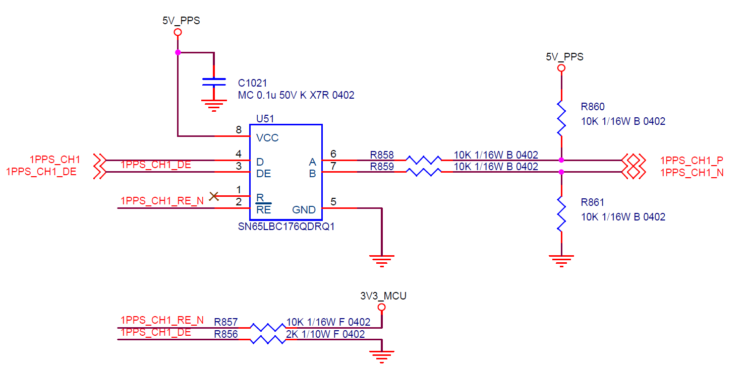
Dear Team,
Please help to double check the schematic.
Is it ok the logic input is from 3.3V MCU and output is 5V logic?
BR
Kevin

