This thread has been locked.

If you have a related question, please click the "Ask a related question" button in the top right corner. The newly created question will be automatically linked to this question.

TUSB320EVM: Oring power diodes in TUSB320 evaluation board

Part Number: TUSB320EVM
Other Parts Discussed in Thread: TUSB320, TPS2121, TPS63020, TPS25910

Hi All

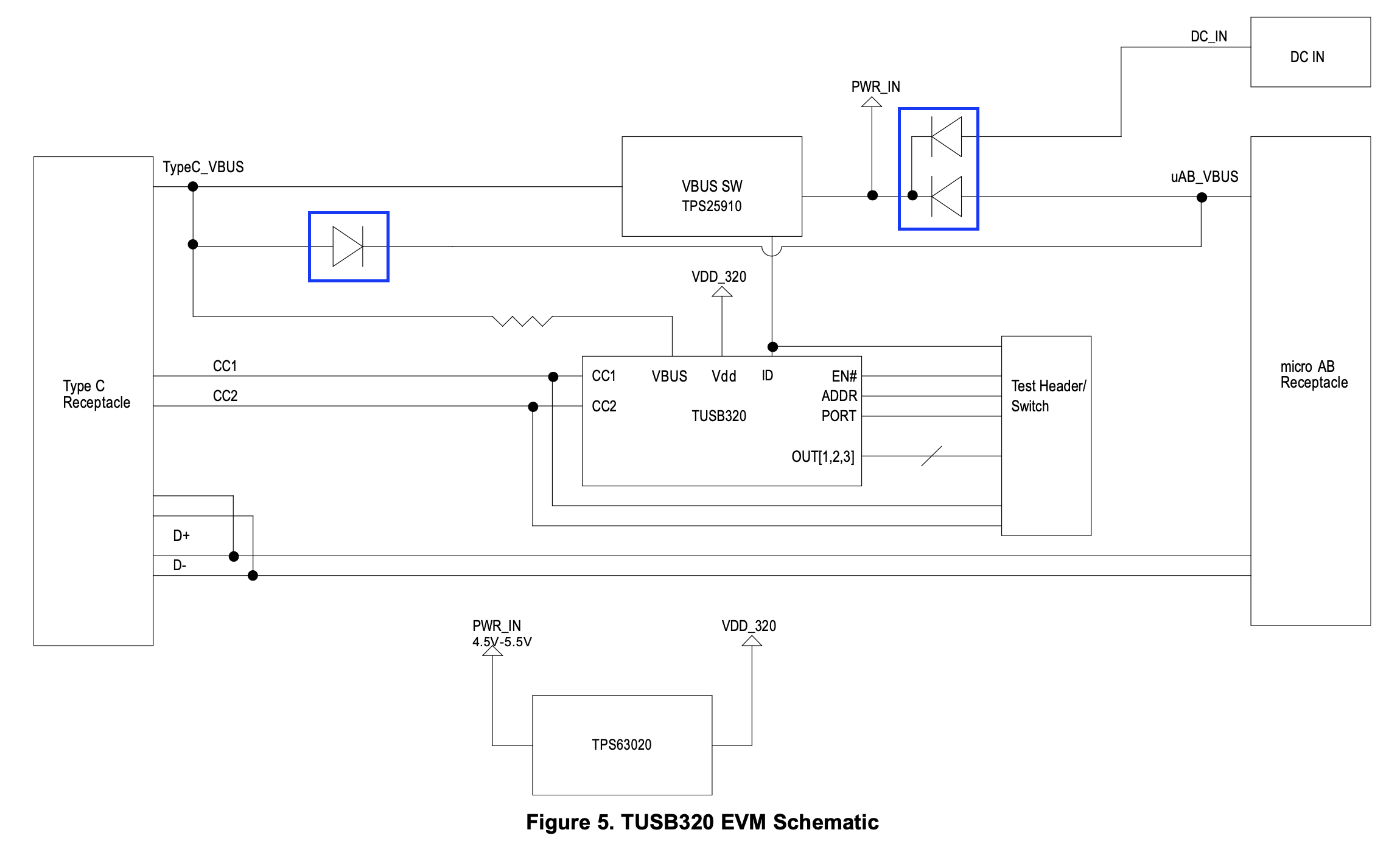
I'm currently evaluating the TUSB320 for a USB Type C project, when looking into the evaluation board schematics I can see Oring power through RB751V-40 diodes, they are highlighted in the screenshot below.

The Datasheet of those diodes mentions current rating of 30mA only.
I was wondering how this could work since the board is rated for 3.0A, while the diodes are only supporting 30mA ?!

Where am I wrong ?
Thanks

  • Hi Jerome,

    The default diodes populated on the EVM are only meant to solely power TUSB320 and basic operation of the TUSB320 (cable detection, TUSB320 I2C read/writes etc.) If you are looking to do actual charging through the EVM the diodes do need to be replaced to handle the load currents seen through Vbus connection. 

  • Thanks for your answer.

    Does this mean I cannot attach a USB Device to the EVM USB-C connector and power it from DC-IN connector if it consumes more than 30mA ? 

  • Correct you will have to replace the diodes in this case. This also assumes that you are connecting to a UFP or Sink device.

  • Thanks

    Would you see a problem using a TPS2121 power mux to replace the Oring diodes, to allow muxing power inputs between DC-In and Vbus ?

    Our block diagram would be in that case your exact TUSB320 EVM (without the Micro AB USB connector), and replacing the Oring diodes with a TPS2121.

  • Hi
    One more question about the TUSB320 EVM.

    The Vdd of TUSB320 comes from a dedicated buck boost TPS63020 converter. This converter generates the VDD_320 (Vdd of TUSB320) from MicroAB Vbus ORed with DC In external jack (Oring Diodes).

    On the board you also have a 3.3V regulator TPS62082DSGT, I do not see anything in the TUSB320 datasheet that prevents from powering the TUSB320 from this 3.3V regulator (Vdd can be as low as 2.7V, and CC1 & CC2pins can be up to 6V without relation to Vdd), why did you add a dedicated TPS63020 only to provide the TUSB320 Vdd rather than using the on board 3.3V regulator ?

    Thanks

  • Hi Jerome,

    The separate power regulator is is to allow for flexibility to change TUSB320 VDD voltage without affecting the rest of the system. TUSB320 can accept 3.3V  VDD so either power regulator could be used. 

    Using a power mux is possible. What would be the second input to the power mux? In other words what would be replacing Vbus from the micro-AB connector?

  • Thanks for the clarification.

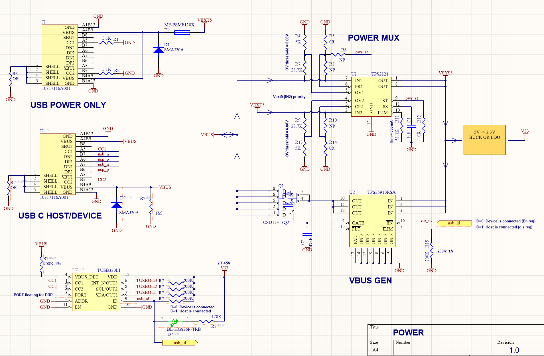
    I attach the schematics, please note all resistors values are not fully calculated yet and there are some missing capacitors, but you will understand the basic idea.

    Basically, we have 2 USB Type C connectors on the board, one is dedicated to power our board when a USB Device is attached, it does not have data connected, it provides VEXT5 to the board.

    The second connector is the USB data/power connector, it provides VBUS to the board when a USB Host is attached.

    USB HOST Attached:

    - VEXT5 is not required, and the board will be powered from the Host, the power Mux will automatically select VBUS as the main supply, or VEXT5 if connected (priority is given to VEXT5), and this will be converted to 3.3V for the electronics.

    - The TPS25910 will be disabled, so no VBUS will be generated by our board.

    USB Device attached : 

    - VEXT5 is required, VEXT5 will be connected to the 3,3V regulator input through the power mux, as well as connected to the TPS25910 input. The TPS25910 will be enabled (with the help of ID pin), and will generate the VBUS to power the attached device.

    - VBUS generated from the TPS25910 will also be present at the power mux IN1 input, but priority is given to IN2 (VEXT5).

    - Question : Should I add a diode between VBUS and IN1, just to be sure the forward voltage of the diode will result in VBUS < VEXT5 and so we are sure the Power Mux out will be IN2 (VEXT5) ?

    Hope this is clear, do you see something that could be wrong in this schematics ?
    Thanks for your help.
    Jerome


  • Hi Jerome,

    I agree with the general idea behind the schematic. I agree with the idea adding the diode to help prevent Vbus > VEXT5 case when a device is connected however you should consider that USB allows some variation in Vbus and can be as low as ~4.75 V (coming form attached power source).

    Power only port will be limited to 500/900 mA current capacity when using only pull down resistors. You should also considering timing of Vbus and ensure that there are no large delays from when USB device is connected and Vbus is present. 

    Note: You can also consider implementing a PD controller and using a power role swap to ensure Vbus flows in the proper direction, potentially reducing the number of ports.

  • Thanks for your answer.

    I added a S1A diode between VBUS and IN1. S1A has 0.9V voltage drop @100mA which corresponds to my MCU and other electronics current consumption.
    Power loss at the diode will be less than 0.1W, which seems acceptable to me.
     
    VBUS range is 4.75V to 5.5V according to the USB spec.

    When a USB Device is attached, and if VEXT5 is 4.75V (Worst case), generated VBUS will be 4.75V (negligible voltage drop in TPS25910) and VIN1 will be around 3.85V (after the diode voltage drop), this should ensure the VEXT5 will be automatically selected as the power source.

    When a Host is attached, if VEXT5 is still present at 4.75V and VBUS is 5.5V (Worst case), VIN1 will be around 4.6V (after the diode voltage drop), this should ensure the VEXT5 will be automatically selected as the power source.

    When a Host is attached, if VEXT5 is no longer present and VBUS is 4.75V (Another worst case), VIN1 will be around 3.85V (after the diode voltage drop), this should ensure the voltage at the mux output is still enough to power the 3.3V LDO

    Yes, I want to limit VBUS to 500mA 5V.

    Regarding timings on VBUS, there is no capacitor connected to VBUS, and the capacitor on the power mux Soft Start pin was reduced to 220nF.
    The LDO has a 47uF load capacitor.

    Thanks again to comment, and thanks again for your great support.
    Jerome.


  • Hi Jerome,

    No problem, you should consider adding some capacitance on Vbus to limit inrush current.