Hi Lee,
We carefully analyzed the model as now comes the critical phase where the CCAs are in-house and we're in the process of evaluating the circuit performance.
Let’s start with a simple time domain simulation in LineSim using the schematics, as given.
(screenshot #1)
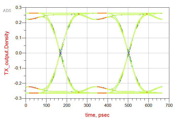
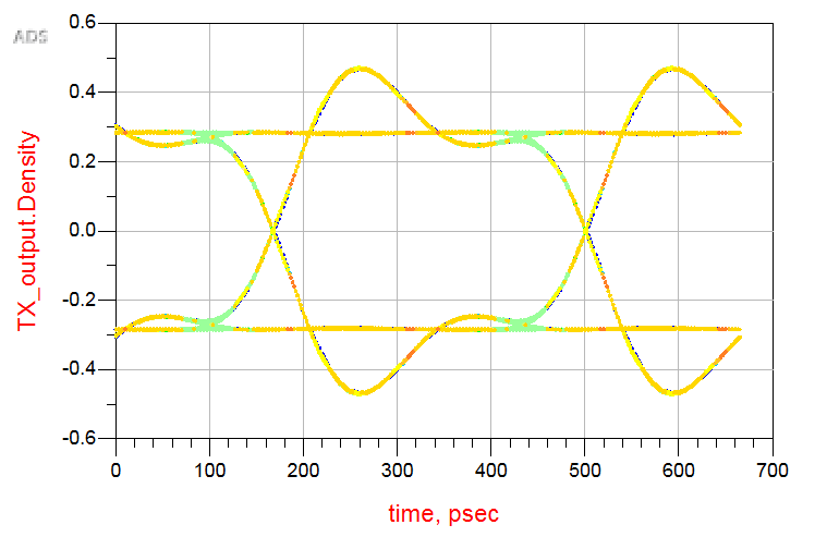
The waveforms at each IBIS model look like this:
(screenshot #2)
Note that the output of the transmitter is lower than expected, 450mV where it supposed to be closer to 900mV.
Note that the waveforms at U2 are basically noise only a few mV in amplitude. Also note that
the waveform at U1 is significantly larger on one of its pins than its other pin. In addition, note
that the waveform on U3.2p is inverted as compared with U1.2, but U3.2n is not inverted of
U1.3. This raises a bunch of questions about J11. Looking at it in the Touchstone viewer, I see
the following:
(screenshot #3)
Note that there is no signal going between the ports that are checked (plotted).
According to the schematics, they seem to expect the main signal path to be
between ports 1 – 2 and ports 3 – 4. The Touchstone file indicates an open between
those ports. Actually when I plot the remaining ports in the Touchstone Viewer,
I see that ports 1 – 3 and 2 – 4 are basically a short, and that there is some non-ideal
connection between the remaining ports:
(screenshot #4TI_SN75LVCP601_IBIS_AMI_Analysis.docx)
So it looks like the port ordering of J11 needs to be changed. I made the same observations
on J12, also.
Now comes the question about U3. The way it’s put on the schematics indicates that
this might be a repeater model of some sort. However, I find no indication in the IBIS
files associated with that symbol that would tell the simulator that the Rx on the left
side of it and the Tx on the right side of it are associated in any way. If this symbol is
indeed a repeater, the IBIS model should indicate that. There are keywords in the IBIS
specification for that.
Finally, It seems that J11, called rx_term, is an S-parameter receiver model for the Rx in U3, and J12 is an S-parameter
driver model for the Tx in U3, along the lines of BIRD158 (or BIRD194), which are actually
included in the v7.0 IBIS specification now. But I find no indication in any of the IBIS files,
or .ami files that would tell me and the simulator that these S-parameter models are
supposed to be serving that purpose. Again, there is an official syntax for all that in
the IBIS spec, and the model files should use that to indicate to the simulator what to
do with these models.
Thanks,
Shalmon