This thread has been locked.

If you have a related question, please click the "Ask a related question" button in the top right corner. The newly created question will be automatically linked to this question.

SN65HVS882: what is spi clk supported by this device

Part Number: SN65HVS882

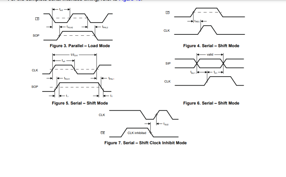
what is spi clk supported by this device and what is DC in below figure??
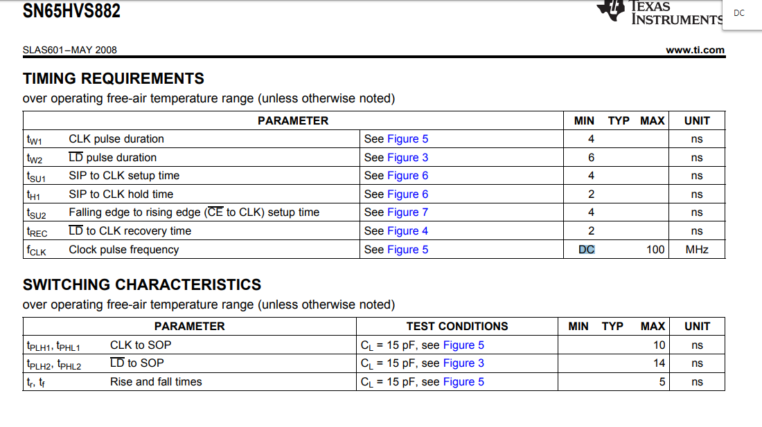
  • Hi Harsh,

    The SPI clock has to meet the minimums shown in the timing requirements for the system.

    Below are the figures explaining the timing parameters:

    There needs to be a minimum of 2 ns of recovery time, t_rec between the time LD hits 50% of its maximum value during its rise time to when the clock pulse reaches 50% of this figure. See Figure 4 for more explanation. LD is similar to the Chip Select line in SPI.

    The minimum clock width, t_w1 shown in figure 5, is 4 ns. 

    The clock pulse frequency, f_clk, needs to be in the range 0Hz - 100MHz, the 0Hz is represented by the value "DC". This is shown in figure 5.

    The clock must also conform the serial input data: the setup time, t_su1, is the minimum time between when the serial input data hits 50% of its maximum value, either rising or falling, and when the clock hits its 50% value on its rising edge, this is shown in figure 6.

    The clock must also hold for a minimum of 2 ns for the input data to be registered as valid, t_H1 shown in figure 6.

    Finally there is another setup time, t_su2, is the minimum time between /CE when it hits its 50% value on the falling edge and when the clock hits its 50% value on the rising edge.

    If the SPI clock you are using can conform to these specifications than it will be okay to use in the application.

    Best,

    Parker Dodson