HI, I have question about USB Super speed or high speed lines.
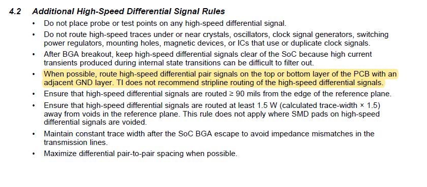
In the document 'TI Highspeed Layout Guide' there says like below.
When possible, route high-speed differential pair signals on the top or bottom layer of the PCB with an
adjacent GND layer. TI does not recommend stripline routing of the high-speed differential signals
--------------------------------------------------------------------
And, I cannot understand why these high speed signals pairs routed in Top or Bottom of the PCB, not stripline.
In my opinion, if I route these speed lines routed as stripline(2nd or 3rd layer in the pcb) and cover with gnd then, it will be more shielded by ground and can be more stronger at emi.
(If like this, then upper and bottom layers are both shielded. )
Top : GND
2nd : High Speed Line
3rd : GND
-----------------
Could you help me why Ti recommends routing high speed signals on the top or bottom?


