This thread has been locked.

If you have a related question, please click the "Ask a related question" button in the top right corner. The newly created question will be automatically linked to this question.

TPS25750: TPS25750 PD Application Question

Part Number: TPS25750
Other Parts Discussed in Thread: TPS62125, TPS562202

We have some application question below.

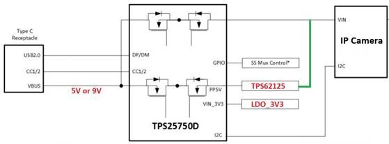
The Type-C input is 9V and 5V, the system load is around 18W.

    1. How to design PP5V and VIN_3V3? Both are need the sequence with VBUS and VBUS-IN.
    1. May I know the TPS25750D muse have PP5V and VIN_3V3?
    1. If yes, May I use TPS62125 buck to 5V for PP5V? and use LDO_3V3 to VIN_3V3?
    1. Do you have reference schematic to share?

BR, Gary

  • Gary,

    I will need to know a little more about the VIN connection in order to fully answer your question. 

    I am going to answer the questions making the following assumption:

    VIN is intended to be used as both and input and output voltage and that it can vary from 5V to 9V.  The system is fully tolerant of VIN ranging from 5V to 9V.

    1,  Figure 9-11 of the datasheet explains the connection of VIN_3V3.  The design will automatically take care of switching between the input VIN_3V3 the VBUS regulator depending on the system needs.  For example: during dead battery, power will be sourced from VBUS to provide LDO_3V3 for IC operation until the rest of the system is sufficiently charged to provide power on VIN_3V3 if it is setup in this manner.  PP5V is an 5V output power path.  The TPS62125 is not sufficient to supply the 1.5A out VBUS current and 100mA VCONN current to meet the minimum type C requirements for this path.  The TPS562202 or some other 2A buck converter is necessary for this path.  You can then utilized a 5V to 3.3V LDO to supply VIN_3V3.  This LDO can be very low current, somthing like 100mA is sufficient.

    2.  PP5V is utilized as the output power path, so if you intend to source powre, then this path is necessary.  If you only intend to sync power, then it is not necessary to provide PP5V or VIN_3V3.

    3.  The Datasheet on-line has includes a reference schematic for the design, but here is a screen capture from 

    I can probably better assist you in answering your question if you provide a higher level block diagram showing what you are trying to accomplish. 

    • Is power always and input from VBUS (18W 9V/2A)
      • If power can be output, what Voltage and Current (5V/1.5A is the minimum here)
    • How is current flow controlled on the VIN pin?

    With a little more information, I can be a lot more helpful.

  • Hi Chuck,

    • The input always from the adaptor (18W 9V/5V@2A). So that we don’t need the source power (PP5V power path), then it is not necessary to provide PP5V and VIN_3V3. Is that correct? If Yes, may I lead the PP5V, VIN_3V3 and VBUS pin to floating?
    • Based on our condition. May I use LDO_3V3 for our system internal use in logical circuit?

    BR,

    Gary

  • PP5V should be connected to ground in this case. 

    VIN_3V3 should still have a 10uF capacitor connected.

    VBUS a VBUS_IN should be shorted together

    LDO_3V3 is very limited in the amount of current that it can support. It is really intended to only power the boot EPROM, not to be a general purpose LDO for the entire system.

    I have marked up the schematic from the datasheet to show the connections.