This thread has been locked.

If you have a related question, please click the "Ask a related question" button in the top right corner. The newly created question will be automatically linked to this question.

SN65HVS882: Does this IC need Power cycle?

Part Number: SN65HVS882

Dear team,

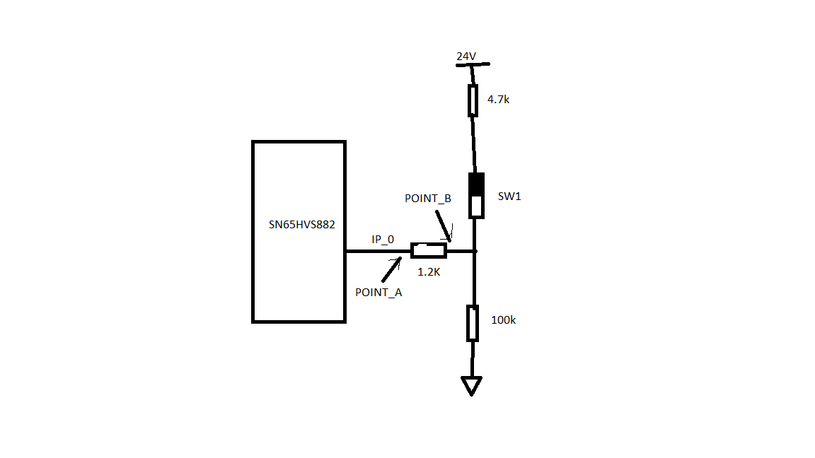
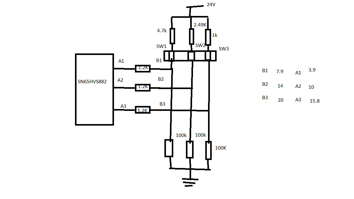
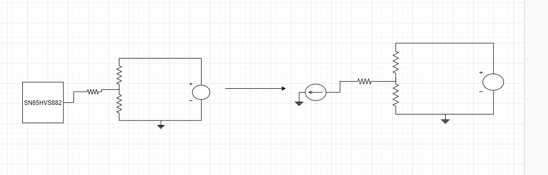
We are using this IC to read data from sensors. we have made testjig where we are feeding 8 digital inputs which is of 24V level to SERIALIZER and we are reading it from SOC. Right now we are only able to read it first time, if we change the input to serializer which is some other value we are not able to read it, But if we again power on and of then we are able to read the proper data.

what is the reason for this.

  • Hi Harsh,

    To clarify the issue that you are seeing is that you have 8 input digital sensors into the field Inputs (IP0-IP7) and the Serial Output (SOP)  is being read by an SOC, and you are only able to shift the first 8 bits into the SOC, then you have to cycle to the power to keep reading more inputs. Am I correct - if not please could you clarify a few things:

    1. What if anything is connected to the Serial Input (SIP) ?

    2. Can you confirm that the sensors are on the field inputs (IP0-IP7) or if they aren't there where they are in the system.

    3. Could you clarify what you mean by change the input to serializer? Do you mean drive /LD High (To terminate parallel loading) and /CE low (To enable clocking)

    Please let me know the above information so I can help you find a solution.

    Best,

    Parker Dodson

  • My circuit looks like as shown

    Case 1: Keep the SW1 on and after power on the ic will read that as 1 i,e(Voltage at POINT A & B respectively 12V and 9V)

    Case 2: Do not turnoff and make sw1 low and after reading data it will be 0,

    case 3: Do not Power of  board agin make SW1 high But IC will read low i,e Voltage at POINT A and B respectively 7V and 3.9V.

    my question is why there is such a voltage drop in 3 rd case. because of that if we change the data input it is not reading properly, It will read correct data only when you Power on for the first time.

    There is nothing connected except the switch, 

    and it is read at SOC via SPI lines. for case 3 we are again loading LD and CS.

  • Hi Harsh,

    Can you clarify what your R_lim value is on the the system?

    Also can you verify that this is the process that you are using:

    Case 1:


    Initial Settings:


    /LD - High (disabled)

    /CE - High (disabled)

    CLK - don't care

    Load Register:

     /LD - Low (enabled)  -> this will override any other control signal on the device and it will load values from the IPx inputs.

    Read Data from SOP:


    /LD - High (disabled) -> this will stop loading bits into the register

    /CE - Low (Enabled) -> Enable Clocking 

    All parallel Bits will be read in 8 Positive clock edges at SOP. After the initial 8 bits have been read the SIP data can be read or /CE can be driven high to disable shifting.

    At the end of Case 1 /LD and /CE can be  high (disabled) to put the device in a no change state until we need to load new data in.

    For CASE 2 and CASE 3 they should follow the same procedure:

    0. /CE and /LD start High - Serializer is in a no - change state

    1. /LD Low - Load Parallel Bits

    2. /LD High - Disable parallel load and drive the device to a no change state

    3. /CE - High - Enable Clocking, all parallel data will be read in 8 positive edges from the clock at the SOP output

    4. After Parallel Data has been read  set /CE - Low - this is to disable clocking when the sensor data has been read without reading in data from SIP which I don't think you are using in this scenario . 

    5. The device now has /LD and /CE high which will put the device into a no change state. When going for the next measurement and /LD goes low the field data will replace the data in the shift register and the process can start again.

    Another thing that sticks out to me is that the current being pulled through the Ip0 input seems to be the same in both cases. That makes me think that there may be a problem somewhere outside of the chip as well. On Case 3 do you have measured voltages from all the nodes listed. I want to make sure there isn't another part of the system that may be causing issues because with the same current being drawn at IP0 I am not sure that it is causing the voltage drop seen in the system.

    Please let me know so we can see if there is some other problem causing the misread.

    Best,

    Parker Dodson

  • Hi Parker Dodson,

    We are using 3.32K of R_LIM resistor,

    and in case 3 in my query Point A and B is 3.9 and 7V respectively.(That was a typo error from me).

    We are  following the proper procedure as we are reading proper data for the first time. It is in only 3rd case where after making SW1 high again the signal input will be 3.9 V which obviously IC will read that as low, 

    My doubt is like will the De-bounce circuit in IP0 pins affects anything?

    This system is not connected to anywhere, where spi lines connected to SOC(MOSI is not connected).

    and on the other side IP pins are connected as per previous diagram.

  • Hi Harsh,

    Please correct me if I am wrong, but do you have both DB0 and DB1 open circuited?

    If this is true you do have the maximum debounce time selected of 3ms. I am not sure if this would directly cause the issue you are seeing - but it could be a possible source. If you can try to Ground DB1 to bypass the filter and re-run the tests. If it is something to do with the debounce filter, bypassing it should prove that is the problem area - but if the same error occurs something else is most likely causing it. You can wait to enable the clock to let the voltages settle if you want to mimic the debounce wait time. If you ground DB0 instead of DB1 the delay may be shortened. I would recommend trying both of those configurations to  see if there are still errors present when attempting to read data. That will help us narrow down possible problem areas.

    Also have you seen this issue present on multiple boards? Have you been able to replicate the problem on multiple boards?

    Please let me know so we can hopefully narrow down some possible issues because the behavior you are experiencing does seem abnormal!

    Best,

    Parker Dodson

  • Dear Parker Dodson,

    Both DB is connected to grond through 0 ohm resistor

    Here in image there are other voltage readings for different Pullup values.

    In 2.49K and  1K pullup Values the voltage does not change after toggling the Switch.

    I was not able to come to the conclusion for the issue? My doubt is the selected resistor is a strong pullup and the supply not able to provide proper required current for sink in 4.7K case? 

  • Hi Harsh,

    So I think the source of your problem is how the DB pins are set. Please refer to the table below:

    When both DB pins are grounded that is a reserved function - so the operation of the device is not going to work as expected. I'd change to one of the other three options and most likely I think this may be causing the issue.

    As for the pull-up values - the reason you see the voltage divider increase with a decrease in the pull up value please see the diagram below:

    The Serializer Field Inputs basically act as a current source (That is set by RLim) - the voltage drop is about equal in all cases you have presented which show that the current source is acting pretty consistently. I don't think that is the source of the problem - I do believe it is because you have grounded both DB pins. Only one should be grounded at most.

    Best,

    Parker Dodson

  • Dear Parker Dodson,

    That did not work....

  • Dear Parker Dodson,

    We have Isolated the 1.2K resistor IC side PAD and checked the Voltage at before and after resistor, the voltages are respectively 24V and 22.8V.

    So when we connect resistor to IC inputs then only we are seeing a Voltage drop.

    Regards

    HARSH

  • Hi Harsh,

    What did you set the DB pins to? Did you have them bypass the debounce filter or did you set a delay? 

    There is going to be a voltage drop between the field side of the resistor and IC side of the resistor, so that isn't an error condition. Please see below:

    They measure the voltage at filed side and IC side - there is supposed to be a voltage drop. The voltage drop is different in your application because you have a different Rlim value than what is specified in the above table.

    For me to help you I am going to need more information, and I need to know the following information to help see if there is an operating condition:

    How is the IC connected - there has been confusion before, like with the DB pins,  what is every pin connected to on the IC.  What is the voltage supply?

    Have you been able to replicate this problem on multiple boards?

    What did you switch the DB configuration to and have you tried multiple settings?

    Please let me know, the more information I have the easier it will be for me to try to find a problem.

    Best,

    Parker Dodson