This thread has been locked.

If you have a related question, please click the "Ask a related question" button in the top right corner. The newly created question will be automatically linked to this question.

PCA9306: Schematic check

Part Number: PCA9306
Other Parts Discussed in Thread: LSF0204, TXS0102

Hi team,

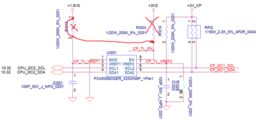
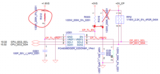
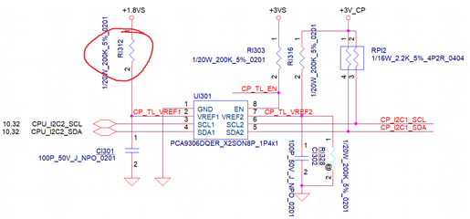
For PCA9306, customer proposed below schematic. Would you please help to review please?

Key concern for customer is +3V_CP comes earlier than +1.8Vs, and +3VS (the EN pin) comes latest. Will there be leakage concern based on this design?

My idea on the schematic is the RI312 200K pull high to 1.8V should be removed, is that understanding correct?

Thanks

Max

  • EN and VREF2 must be connected together (and there must not be a pull-down resistor). VREF1 must be connected directly to 1.8 V. During normal operation, a leakage current flows into VRFEF2 and out of VREF1.

    With the correct circuit, there is no leakage current if the 1.8 V supply powers up first.

  • Thanks for the help Clemens!

    Max,

    I've notified an applications engineer of this thread and they will be responding accordingly.

    Regards,

    Eric Hackett 

  • Hi Max,

    Here is my schematic review:

    Schematic Pinout matches datasheet pinout: Correct

    Decoupling Capacitors : Correct

    SCL and SDA lines Match: Correct

    EN Pin: The set up that Clemens is referring to can be seen below. This setup should be used when VREF1 does not equal VREF2.

    What is required about this setup is that the VREF2 pin is not directly connected to VCC2. VREF2 is required to have a pull up resistor and as Clemens said the pull down resistor (RI328) should be removed. I would like to point out that you do not need to connect the EN pin to VREF2 if you would like to use this device in a switch configuration where VREF1=VREF2. This is an example circuit of the Switch configuration.

    Keep in mind that you cannot use this configuration since VREF1 does not equal VREF2 so as Clemens stated you should use the translation configuration and have the EN pin connected to VREF2. 

    As you stated RI312 should be removed. VREF1 can be connected directly to VCC1.

    There should be pull up resistors on all SDA and SCL lines. Have you checked to see if they exceed the maximum resistance value?

    Lastly, as Clemens said there is a leakage current that flows from VREF2 to VREF1. Section 8.1.7 talks about how this could cause issues if and LDO is used to power VREF1. If that is the case for your system refer to section 8.1.7 in order to calculate the value of a weak pull down resistor that can be placed on VREF1.

    If VREF1 is powered before VREF2 then there should be no leakage current.

    Best,

    Chris

  • Hi Chris, and team,

    Really appreciate your detailed explanation. 

    One more question which your last statement, our plan is to connect 3.3V rails on VRef2 side and it will comes earlier then 1.8V voltage rail on Vref1. The plan is to connect EN to 1.8V directly. Could you help to confirm if it is the correct move?

    Thanks

    Max

  • I add in the capture to help understanding my description.

  • Sorry I just remembered the previous discussion in previous E2E thread https://e2e.ti.com/support/interface/f/interface-forum/984303/pca9306-pca9036-application-question?tisearch=e2e-sitesearch&keymatch=pca9306# 

    So I think the schematic change in the last message is not right, please help to confirm.

    So based on current discussion, please review my below statements, 

    *** back ground is 1.8V VRef1 rise later than 3.3V VRef2 and we want to prevent leakage from 3.3V to 1.8V ***

    1. The GPIO control of EN pin is not applicable because the Vref1 and Vref2 have different voltage ratings.

    2. EN and 200K resistor are supposed to be connected together and pulled up to the higher voltage.

    3. In my current application, since the lower voltage (1.8V) comes later than the higher voltage (3.3V), to prevent the leakage, we should not connect the EN to 3.3V reference.

    4. Due to the limitations mentioned in previous 3 claim, do you think below design is the only approach here? 

    5. Do you think LSF0204 maybe the better option if customer insist on have a separate enable control pin by GPIO?

    Thanks for your help.

    Max

  • When the higher voltage (3.3 V) powers up first, then the leakage current can partially power up the other supply, which is probably not what you want.

    1. Yes. (EN could be pulled low with an open-drain driver, but that is not possible without power.)

    2. Yes.

    3. Correct.

    4. This would work. (As long as the EN voltage is not above the I/O voltages, no current flows.)

    5. The LSF0204 would work, but the TXS0102 would be a simpler solution.

  • Hi Clemens, 

    Thank you for your reply. 

    One last question that, if customer want to use the EN pin, do you think below schematic could work? (To connect EN and Vref2 together and pulled to EN power rail.) Still 3.3V comes earliest then 1.8V, and the EN pin comes last. 

    If it could work what will be the Pros and Cons compared with the previous one that leave Vref1 and Vref2 pin disconnected?

    Thank you 

    Max

  • This schematic still shows a pull-down at the EN/VREF2 pins. Assuming it is not present, this will work: while EN is low, no leakage occurs.

    In the previous circuit without VREF1/VREF2, EN must be driven to 1.8 V. In this circuit, EN must be driven with an open-drain output. (A third alternative is to drive the other end of the 200 kΩ resistor with a 3.3 V push/pull output.) Which one to choose depends on what is connected to CP_TL_EN.