This thread has been locked.

If you have a related question, please click the "Ask a related question" button in the top right corner. The newly created question will be automatically linked to this question.

TMDS181: Register 0x20 Bit[7] Read always Power Down question

Part Number: TMDS181

Hello.

We have a project used TMDS181 on source side. We Read 0x20 Bit[7] always  is 1 (Power Down) and check OE pin status is high.

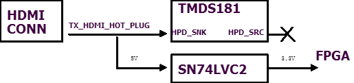
Below is schematic and Register for you reference. Please kindly help comment which Register need be changed. Thanks~

[Mon Jan 22 18:37:01.010 2018] (32) ADDR: 0 DATA: 54

[Mon Jan 22 18:37:01.032 2018] (32) ADDR: 1 DATA: 4D

[Mon Jan 22 18:37:01.056 2018] (32) ADDR: 2 DATA: 44

[Mon Jan 22 18:37:01.081 2018] (32) ADDR: 3 DATA: 53

[Mon Jan 22 18:37:01.104 2018] (32) ADDR: 4 DATA: 31

[Mon Jan 22 18:37:01.128 2018] (32) ADDR: 5 DATA: 38

[Mon Jan 22 18:37:01.155 2018] (32) ADDR: 6 DATA: 31

[Mon Jan 22 18:37:01.177 2018] (32) ADDR: 7 DATA: 20

[Mon Jan 22 18:37:01.201 2018] (32) ADDR: 8 DATA: 1

[Mon Jan 22 18:37:01.222 2018] (32) ADDR: 9 DATA: 2

[Mon Jan 22 18:37:01.245 2018] (32) ADDR: A DATA: 31

[Mon Jan 22 18:37:01.269 2018] (32) ADDR: B DATA: 0

[Mon Jan 22 18:37:01.291 2018] (32) ADDR: C DATA: 0

[Mon Jan 22 18:37:01.315 2018] (32) ADDR: D DATA: 3E

[Mon Jan 22 18:37:01.338 2018] (32) ADDR: E DATA: 0

[Mon Jan 22 18:37:01.361 2018] (32) ADDR: F DATA: F

[Mon Jan 22 18:37:01.387 2018] (32) ADDR: 10 DATA: 0

[Mon Jan 22 18:37:01.408 2018] (32) ADDR: 11 DATA: 0

[Mon Jan 22 18:37:01.432 2018] (32) ADDR: 12 DATA: 0

[Mon Jan 22 18:37:01.456 2018] (32) ADDR: 13 DATA: 0

[Mon Jan 22 18:37:01.480 2018] (32) ADDR: 14 DATA: 0

[Mon Jan 22 18:37:01.504 2018] (32) ADDR: 15 DATA: 80

[Mon Jan 22 18:37:01.529 2018] (32) ADDR: 16 DATA: 0

[Mon Jan 22 18:37:01.555 2018] (32) ADDR: 17 DATA: 0

[Mon Jan 22 18:37:01.577 2018] (32) ADDR: 18 DATA: 0

[Mon Jan 22 18:37:01.601 2018] (32) ADDR: 19 DATA: 0

[Mon Jan 22 18:37:01.625 2018] (32) ADDR: 1A DATA: 0

[Mon Jan 22 18:37:01.649 2018] (32) ADDR: 1B DATA: 0

[Mon Jan 22 18:37:01.672 2018] (32) ADDR: 1C DATA: 0

[Mon Jan 22 18:37:01.697 2018] (32) ADDR: 1D DATA: 0

[Mon Jan 22 18:37:01.720 2018] (32) ADDR: 1E DATA: 10

[Mon Jan 22 18:37:01.746 2018] (32) ADDR: 1F DATA: 4

[Mon Jan 22 18:37:01.769 2018] (32) ADDR: 20 DATA: E8

  • Hello AJ

    Can you confirm which mode are you using? is I2C or GPIO mode?

    Regards
    Francisco
  • Dear Francisco.

    Sorry. These settings Is on I2C mode.

    We forget to update the schematic. Thanks~

  • Hello AJ

    It means that you have another schematic version? Can you upload?

    Regards

    Francisco

  • Dear Francisco.

    I got new schematic for you reference. Please kindly provide your suggestion and thanks for kindly help~

  • Hello AJ

    I send you my comments regarding your schematic:

    - We recommend starting with .2uF capacitor on OE pin, but 1uF is ok.
    - We recommend using a 7.06k at Vsadj pin as the first option value.
    - We recommend using a 500 k at SPDIF_IN if not needed, if you won't use it, then ARC_OUT have to be let floated.
    - Will you use the DDC as source application? if so, you have to use 2 k pull-ups at SCL/SDA_SNK/SRC pins.
    - The HPD_SNK has to be connected to the sink and HPD_SRC to the source. If you connect the HPD_SRC to the source, you have to be sure that the voltage levels are correct, if not, you have to use a level shifter.
    - When you are using the I2C, pin 21 (EQ_SEL/A0) is used as part of the I2C programation.
    - The Test/A1 pin is not connected, in this case, you are using the I2C mode, then you have to put a level on this pin according to your configuration. For more information, please take a look at the datasheet.
    - The pin 40 is NC, the connection is correct, but your diagram looks like this pin has a functionality.
    - We also recommend using 65k pull-up/down resistors for configuration pins.

    Please, do all of these changes and perform a double check on the datasheet for pins like A0, A1 functionality.

    Regards
    Francisco
  • Dear Francisco.
    Thanks for you kindly suggestion. We will follow and try it. Thanks~
  • Dear Francisco.

    Update on below for you reference. But still got same problem. Please kindly help provide your suggestion.

    By the way. If change to DP159 is better than TMDS181 or not? Thanks~

    - We recommend starting with .2uF capacitor on OE pin, but 1uF is ok.

    We used 1uF.

    - We recommend using a 7.06k at Vsadj pin as the first option value.

    We used 6.98K.

    - We recommend using a 500 k at SPDIF_IN if not needed, if you won't use it, then ARC_OUT have to be let floated.

    We used 499K.

    - Will you use the DDC as source application? if so, you have to use 2 k pull-ups at SCL/SDA_SNK/SRC pins.

    SCL/SDA_SNK/SRC have been used 2 k pull-ups

    - The HPD_SNK has to be connected to the sink and HPD_SRC to the source. If you connect the HPD_SRC to the source, you have to be sure that the voltage levels are correct, if not, you have to use a level shifter.

    The HPD_SRC of TMDS181 do not use for our design and pin 19 of HDMI  contact to both HPD_SNK of TMDS181 and SN74LVC2(level shifter) as below diagram

    - When you are using the I2C, pin 21 (EQ_SEL/A0) is used as part of the I2C programation.

    We are using in I2C mode

    - The Test/A1 pin is not connected, in this case, you are using the I2C mode, then you have to put a level on this pin according to your configuration. For more information, please take a look at the datasheet.

    Both A1 and A0 pull down to ground through resistor 63.4k ohm

    - The pin 40 is NC, the connection is correct, but your diagram looks like this pin has a functionality.

    The Input lane SWAP function don’t use

    - We also recommend using 65k pull-up/down resistors for configuration pins.

    We will change the resistor

  • Hello AJ

    Can you upload your diagram? I would like to see the changes that you did and also, can you confirm if the voltage sequence is correct? if possible, please upload a scope measure. The TMDS181 is designed to handle HDMI, then this is the best option for your application.
    Can you confirm if the HPD_SNK has the correct voltage level?
    Can you confirm if you are using the correct address for the I2C lecture? For your configuration, the w=BC and r=BD.
    In your diagram, the pin 40 is named as SLEW_CTL and this pin in the chip is not connected, that's what I mean.

    Regards
    Francisco