This thread has been locked.

If you have a related question, please click the "Ask a related question" button in the top right corner. The newly created question will be automatically linked to this question.

TCA9534: TCA9534DWR SDA issue

Part Number: TCA9534

Hello Team,

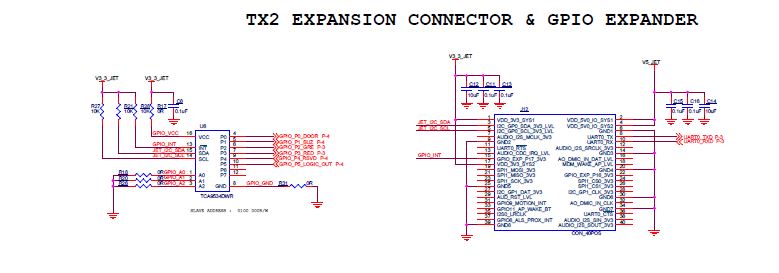
I am using TCA9534DWR GPIO expander, its voltage rail is 3.3V, and I2C is pull up(3.3v) with 10K resistor. Which is power by using Jetson TX2 developer kit. But after some use its SDA pin shows ground potential and also reduced the impedance b/w VCC and Gnd. The issue was solved when we replaced current chip with new one .What was the reason behind the issue, please support.

Regards,

Jiffin

  • Hey Jiffin,

    This question is a bit difficult for us to answer with just the information provided.

    1) Can you provide a schematic of the set up you used when the device broke?

    2) Can you provide waveforms of when you communicate with the device?

    3) After replacing the device, has the new device seen the same damage after uses?

    4) What was the ambient temperature you were testing this device at? (were you cycling different temperatures? or was this tested at room temp?)

    5) Is this something that occurred only once? (1 board and 1 device or multiple boards and multiple devices?)

    My current thought on this is if after replacing the device and seeing the new device work properly without being damaged then the issue was likely related to ESD or EOS. Another thought is the device could have been damaged during the soldering process the first time.

    Now if the device breaks again after multiple uses then I believe we need to take a closer look at the schematic/layout to find the root cause.

    Thanks,

    -Bobby

  • Hello Bobby,

    Thank you for your reply, Please find the schematic shared above. Currently we don't have any waveform to share with you. we just replaced the IC till now there is no issues. We are tested in room temperature and same issue occurs in another board also. 

    Regards,

    Jiffin  

  • Hey Jiffin,

    Your schematic does not show anything that looks like it would immediately damage the SDA line. This is assuming the master (Device on the right) uses an open drain architecture on its "I2C_GPIO_SDA/SCL" line. If it is using push pull then what we would see is the device would actually see an excessive amount of current on the 9th clock cycle and damage the TCA9534 device when it ACKs (this will occur only to SDA). This damage may occur after a few ACKs and not on just the first ACK. A scope-shot would confirm this because the VoL during the ACK would be abnormally large (maybe around 30% of Vcc or even higher) and the clock and SDA rise times will look fast due to the push pull and the waveforms would look like a square wave. I would recommend you hook it up to the scope if you are unsure or double check the datasheet on the master.

    I've looked into our quality return database on this device and found there have been zero returns due to quality issues. (I did this to check to see if other customers have seen the same issue you saw the first time around.)

    For now, if you have tested the TCA9534 multiple times and have verified on the scope that the device is not seeing the abnormally large VoL on the 9th clock cycle then I believe the first devices were damaged during the assembly phase as it seems you have seen this issue on more than one board. Please feel free to post the o-scope shots online here for us to verify as well.

    If you still have the "faulty" devices from the first go around, you can contact the distributor you got our devices from and have them send the devices back for a quality check if this is still a concern. If you worked with an FAE (Field Applications Engineer) from TI, then I believe you can also contact them about a quality concern and work with them to initialize a quality check with our quality engineers.

    Thanks,

    -Bobby

    Side Note: we typically recommend not to leave unused GPIO pins floating. I don't believe this is the reason for the SDA seeing damage the first time around but will likely cause more supply current to be drawn from the device.

  • Hello Bobby,

    Thank you for your response,  Master on the other side is NVDIA's Jetson TX2 development Kit. In the datasheet of Jetson TX2 it is mention that the SDA / SCL lines are open drain and also for i2c configuration SDA/SCL lines are never be in push pull configuration. Is there any possibility to design an architecture with SDA as push pull, which is opposed to the I2C architecture

    For your reference  NVDIA's Jetson TX2  datasheet attached.

    We also noticed that, the pull up resistor on the SDA line will reduced to 1K from 10K. when the chip fails. Do you have any clue for this problem.

    Regards

    JiffinJetsonTX1_TX2_Developer_Kit_Carrier_Board_Specification1.pdf

  • Hey Jiffin,

    "Is there any possibility to design an architecture with SDA as push pull, which is opposed to the I2C architecture"
    1) There are two ways for me to interpret your question here, the first is if you are purposely trying to make this device such that SDA can support a push pull. SDA of our device basically has an input stage where it uses digital logic to determine if the signal is high or low (this stage is seen as high impedance) and a output stage that uses a FET to pull low. You do not want to place SDA in line with a push pull architecture because if another device pulls high with a FET (low impedance) and our device pulls low with our pull down FET, what we have is a path from Vcc to GND with two low impedances in series which look like a short circuit and our pull down FET could be damaged by this large current.

    2) The second way I can interpret this question is there is another way for a push pull connection to be accidentally connected to our SDA pin. The only time I see this is when a designer uses an FPGA and is not aware the output pins should not be actively pulled high by the FPGA. I have seen this happen once or twice before.

    There is another way I can think of the SDA being damaged, and that would be using an I2C switch with a lot of channels enabled using strong pull ups. I am assuming the only I2C devices connected to this are the master and our IO expander so this is likely not the problem.

    "We also noticed that, the pull up resistor on the SDA line will reduced to 1K from 10K. when the chip fails. Do you have any clue for this problem."
    -What do you mean by fail? The device breaks or you get a NACK? Too much resistance can cause the rise time of the SDA/SCL signals to be too slow and affect signal integrity and if resistance is too low then when the master pulls low, the VoL could be larger than 30% of Vcc and not be interpreted as a low by the slave. 1K to me seems like it should not cause the VoL issue or damage the device..... Could the PCB our device is on be shorted somewhere?

    It would be easier for me look at the o-scope for the SDA and SCL lines of the device to really see what is going on.

    Additional questions:
    A) Is it possible you are connecting the wrong outputs of your Jetson TX2 to our device? (maybe one that uses a push pull set up?)
    B) Is our device being communicated with through jumper cables from the Jetson TX2?
    C) I noticed that the datasheet of the Jetson has a level shifter (J24), is the voltage actually 3.3V or is it shifted?

    Thanks,
    -Bobby