Other Parts Discussed in Thread: TCA9517
Hello,
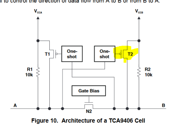
I'm using the TCA9406 with strange behavior that I don't understand.
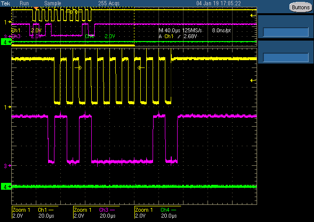
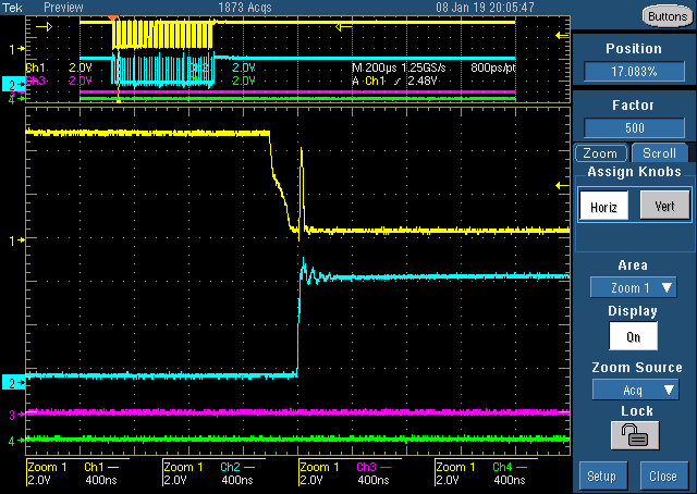
The 9406 is on the slave board. The VCCB (5V) is on the connector side of the slave board. The Master is wired into the slave board. The master board has 2k pull-ups. The VCCA (3.3V) is connected to an FPGA.
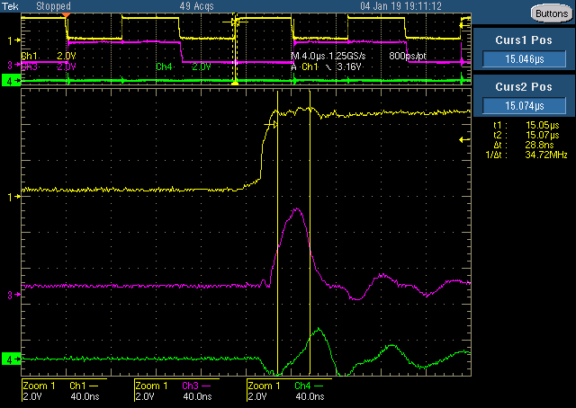
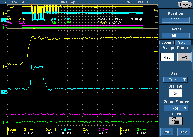
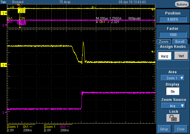
On the B-side I see the master clock and data but there are boards where either the clock or the data aren't getting driven fully low. Some boards have a full swing on the clock but the data is switching only 1/2 scale. Other boards it is just the opposite.
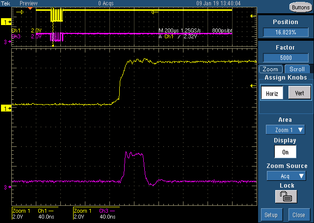
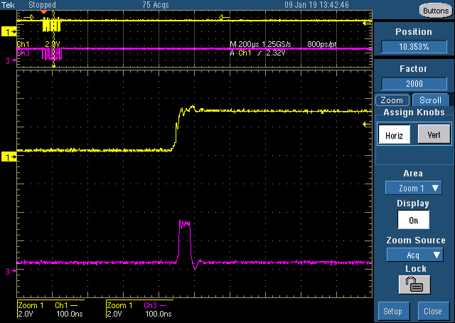
On the A-side nothing comes out of the chip. the SDA_A and SCL_A lines are in a high state. I'm using the 9406 initernal pull-ups on the A-side. There are no external pull-ups on the A-side.
Any ideas?
Rob