This thread has been locked.

If you have a related question, please click the "Ask a related question" button in the top right corner. The newly created question will be automatically linked to this question.

TCA9617B: TCA9617A/B rising time

Part Number: TCA9617B
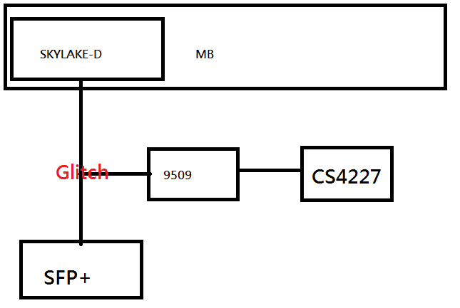
Other Parts Discussed in Thread: TCA9617A, TCA9509

Hello Sirs,

Need your comment .

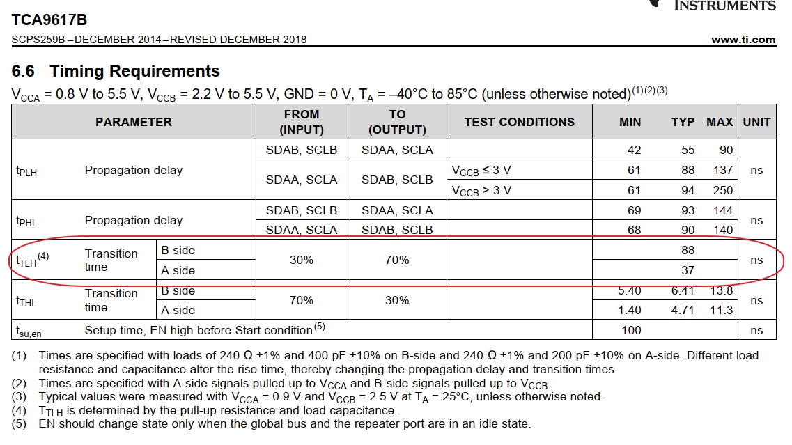
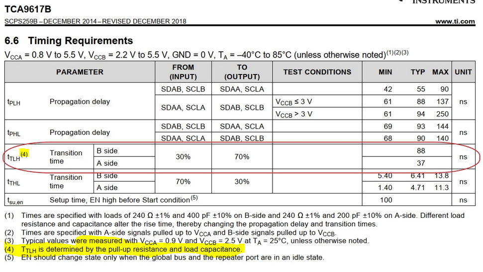
Refer to TCA9617B datasheet 8.3.2 and 6.6 Timing requirements,

- What's the problem if  rising time too fast like attach waveform (B side & 100K pull up resistor) ?

- As waveform , there's a overshoot once the pedestal voltage setup . How to eliminate it ?

Many thanks !

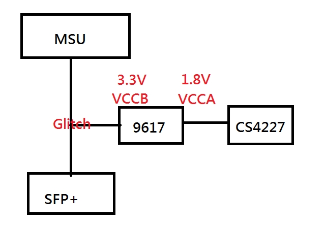
Due to nature of the B-side pedestal and the static offset voltage, there will be a slight overshoot as the B-side
rises from being externally driven low to the 0.5 V offset. The TCA9617B is designed to control this behavior
provided the system is designed with rise times greater than 20 ns. Therefore, care should be taken to limit the
pull-up strength when devices with rise time accelerators are present on the B side. Excessive overshoot on the
B-side pedestal may cause devices with rise time accelerators to trip prematurely if the overshoot is more than
accelerator thresholds. Since the A-side does not have a static offset low voltage, no pedestal is seen on the Aside as shown in Figure 7.


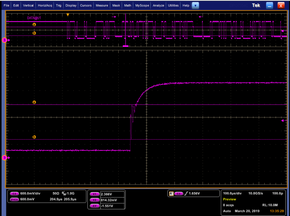
Zoom in to see more detail rising time:


  • Hey Terry,

    "What's the problem if  rising time too fast like attach waveform (B side & 100K pull up resistor) ?"

    That rise time does not look like a 100k pull up. It is likely you are using a device that uses a rise time accelerator if you actually are using a 100k pull up.

    "As waveform , there's a overshoot once the pedestal voltage setup . How to eliminate it ?"

    This is typically due to a strong pull up or low bus capacitance. What you would normally do is make the pull up resistor weaker (larger value) or add some capacitance to the bus. In this case though, it seems like you are using a device with a rise time accelerator. If this is true, then it will likely require a redesign.

    Can you provide a block diagram of your I2C bus? What device are you using with a rise time accelerator?

    Also, you included pictures rise times from the datasheet. But this only shows the expected rise time for a given load condition:

    This kind of information is dependent on the bus capacitance and pull up resistor. It does not take into account a rise time accelerator.

    Thanks

    -Bobby

  • Hello Bobby,

    This is system block . I2C host is in B side 3.3V . TKS !

  • Hey Terry,

    Does either the MSU or the SFP+ have a rise time accelerator? Or is the master driving using a push pull architecture?

    Can you provide me with a datasheet for the MSU and SFP+?

    Thanks,
    -Bobby
  • Hi Sirs

    I have some questions about TCA9617A and TCA9509D.
    As Terry said before, We used TCA9617A first, and there has glitch issue.
    And we change part to TCA9509D, it can fix glitch issue.

    But there are some other issues need to be cleared.

    (1) As pic1, yellow line is SCL(B), purple line is SDA(B).
    There has triangle wave after 9th clk, is it normal?
    We think that it does not affect the reading of the next data.

    (2) After this triangel wave, and next data is high, rise time of this data is 563ns(criteria is 300ns).
    Rise time fail because of triangel wave. (As pic2, pic3)
    Do you have any comments about this?

    (3) We find that undershoot fail on each ACK bit as pic4.
    We find SPEC pic as pic5, there is show SDA would < 0V on ack bit.
    Is it normal? any criteria for this undershoot? Or we plan to add CAP to fine tune this issue.

    (4) What is root cause for TCA9617A glitch issue? Why TCA9509D is better?

    Many thanks.

  • Hey User,

    "There has triangle wave after 9th clk, is it normal?"

    That triangle means that no one is controlling the bus, the signal is being driven high by the pull up resistor. The signal gets pulled low (likely by the master) and that is when the master takes control of the bus again. It's basically a delay between when the slave releases the bus and the master takes control of the bus. I don't see this as a problem unless it is violating a set up timing defined by I2C standard.

    "(2) After this triangel wave, and next data is high, rise time of this data is 563ns(criteria is 300ns).
    Rise time fail because of triangel wave. (As pic2, pic3)
    Do you have any comments about this?"

    The pull up strength on this side is too weak. The RC constant is making the rise time slower. You need to increase the pull up strength.

    I do see a weird pull up at 2.9V, something takes control of the bus and drives the line high, which should not be allowed because I2C is an open drain system. On SCL with no slaves supporting clock stretching, this could be allowable but not for SDA.

    "(3) We find that undershoot fail on each ACK bit as pic4.
    We find SPEC pic as pic5, there is show SDA would < 0V on ack bit.
    Is it normal? any criteria for this undershoot? Or we plan to add CAP to fine tune this issue."

    If the drive strength of a master/slave is really strong, it can generate large undershoots (large di/dt working with parasitic inductance). This undershoot does look to be a concern to me as it shoots below -1V which is outside the absolute maximum allowed. I would be worried the device make break (or the CPU could break as well) over time due to many undershoots.

    "(4) What is root cause for TCA9617A glitch issue? Why TCA9509D is better?"

    The issue with TCA9617A is due to a strong pull up strength on B side resulting in the overshoot glitch.

    TCA9509 and TCA9617A are completely different devices. B side of the TCA9509 does not have a static voltage offset and it's feedback loop works differently.

    --------------

    The waveforms you are showing me seem to indicate there is something on the bus actively driving the signal high which should not be happening on the SDA line. You can see this in picture 4 where the device has these steps at around 700mV. B side of TCA9509 should not have steps (A side should have steps). I believe some kind of contention could be happening between the device and whatever is driving the line high.

    Thanks,

    -Bobby

  • Hi Bobby,

    Thanks for your useful comments!

    For triangel wave(rise time), I change Pull-up RES to 1K from 10K for SCL(B),SDA(B).
    For undershoot, I add Damping-RES(33R) at SDA(B) side).

    But there is a issue about glitch or monotonic when 1st clock high as picture for SDA(B).(About 1.66V)
    Is it normal? Do you have any comments about this issue?

    Thank you.

  • Hey User,

    The signal looks much better now. The first image you showed looks like the SCL line is coupling signals into SDA. THis is not a problem as I2C is robust enough to handle this. The problem is on the PCB you routed SDA close to SCL so the signals can jump from one trace to the other. You can see that everytime SCL goes high or low, SDA swings up or down a little.

    "For triangel wave(rise time), I change Pull-up RES to 1K from 10K for SCL(B),SDA(B).
    For undershoot, I add Damping-RES(33R) at SDA(B) side)."
    You may want to try 20k for the pull up and 50 ohms for the damping. This will help with the crosstalk we see in the first picture you show.

    "But there is a issue about glitch or monotonic when 1st clock high as picture for SDA(B)."
    The stuff on SDA look okay but the purple waveform seems strange. Can you show me both SDA sides and SCL sides in the same picture. I think the issue is still crosstalk but I can't tell, it could be an issue with the RTAs fighting with one of the sides on the 9th clock cycle. (a guess)

    Thanks,
    -Bobby
  • Hi Bobby,
    I have tried to change pull-up RES to 20K, but there will be functional error.
    SO the config at SDA(B) is pull-up=1K, damping=50R , SCL(B) is pull-up-1K(no damping)now.

    About monotonic waveform:

    The first pic's SDA is about 0.8us to the next SCL
    The 2nd pic is pic1's zoom in.
    The 3rd pic is zoom in to see the monotonic, this oscilloscope is 1G only, real waveform is like purple line as before.
    The 4 is also monotonic when falling.

    Is this also normal? Thank you.

  • Hey User,

    I've seen something similar to this before.

    Is there a levelshifter/pass-fet anywhere in your I2C bus infront of the device?

    How long is your communication line?

    "Is this also normal?"

    To me, this doesn't look normal. It looks like something on the bus is causing this to happen (I don't think its our device but something else on the bus).

    Are you able to provide an I2C block diagram of the I2C bus?

    Thanks,

    -Bobby

    Edit: Can you provide a schematic/layout for me to review offline? duynguyen@ti.com

  • Hi Bobby,

    The design document I sent to you.

    Problem IC is U8. (we rework TCA9509 at U8)

    I2C signal is form MB(SKYLAKE-D) thru JOCP1.

    The length at MB is about 5000mil, The length at subcard is about 6000mil.

    And I am really sure that SMBUS(I2C_SCL_SFP0) is connected to this subcard directly from MB, and I put pull-up RES at MB.

    Thank you.

  • It looks like this has been concluded offline so I will be closing this thread.

    If you have any further questions, lets discuss through another e2e post or further through here.
    Thanks,
    -Bobby