This thread has been locked.

If you have a related question, please click the "Ask a related question" button in the top right corner. The newly created question will be automatically linked to this question.

TRS3232: Absolute maximum rating for terminals C1 +, C1-, C2 +, C2-.

Part Number: TRS3232
Other Parts Discussed in Thread: MAX3232, , , TRSF3232

Dear all,

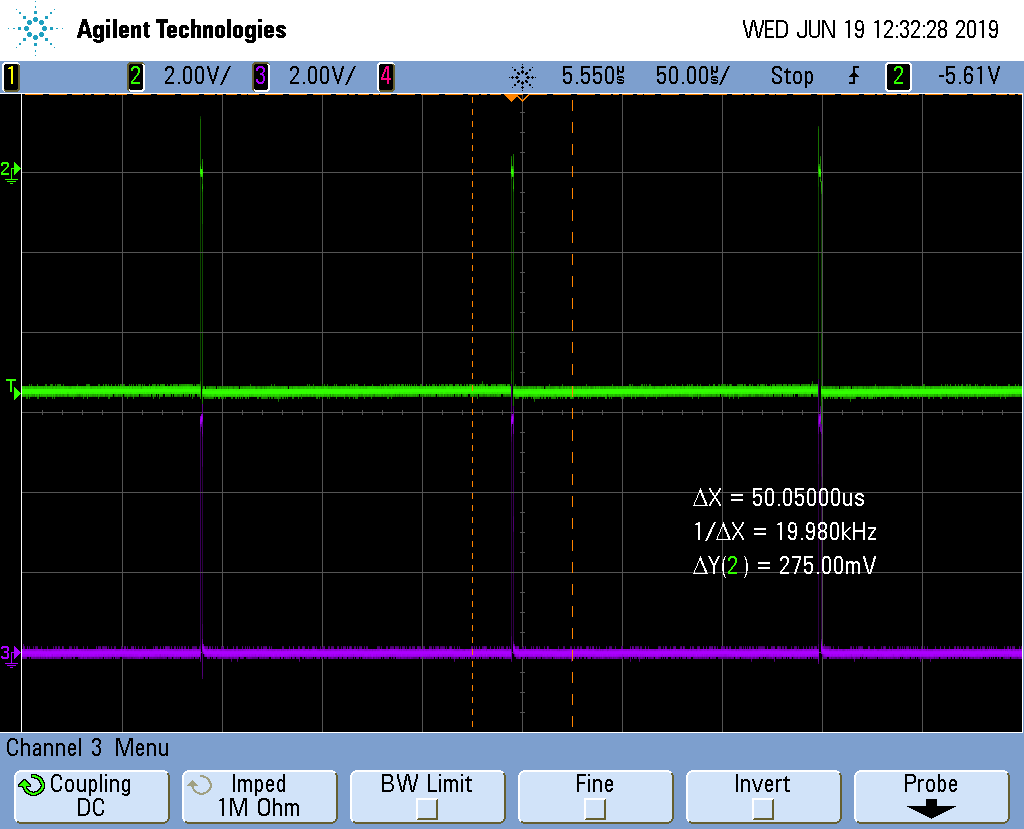
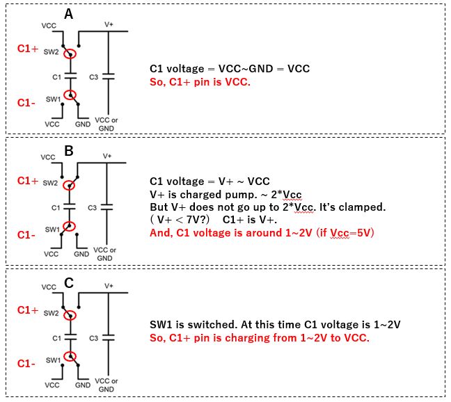
Our customer would like to ask the value of absolute maximum rating for terminals C1 +, C1-, C2 +, C2-.

However, I could not confirm the these value in datasheet.

Could you tell me the maximum rating values for these four terminals?

Best Regards,

Y.Ottey

  • Hello,

    We will work to confirm these values, but due to some critical team members' absences it may take a little longer than usual.  We should be able to provide an update by the end of the week.  Thank you for your patience.

    Regards,
    Max

  • Dear Max,

    Thank you for your reply.

    The customer is urged to answer quickly.

    I would appreciate it if you could get back to me right away.

    Regards,

    Y.Ottey

  • Hi,

    There is no official document about the abs max values of these pins connecting external capacitors. However after some investigation, I think you can treat C1N, C1P and C2P as V+ (7V abs max), C2N as V- (-7V abs max). Please let me know if you have more questions.

    Regards,

    Hao 

  • Dear Hao,

    Thank you for your reply.

    I recognized from the following MAX3232 posts that the absolute maximum rating of these pins is ± 2 x Vcc,

    but can I think that is not the case?

    Regards,

    Y.Ottey

  • Hi,

    It's a good question. Theoretically the output voltage of the charge pump could reach 2x Vcc. However, it's common to limit the voltage range below the abs max, while the voltage level still meets the ±5V minimum of RS-232 standard. You can refer to this post for some detail of the circuit operation.

    e2e.ti.com/.../how-the-rs-232-transceiver-s-regulated-charge-pump-circuitry-works

    Regards,

    Hao

  • Dear Hao,

    Thank you for your reply.

    I am very grateful to you for the materials.

    I would like to ask more question.

    If SW3 and SW4 are switched from this state in the red frame of the circuit in the document (Figure.1),

    is it possible that SW4 becomes V + and SW3 becomes V- due to the difference between the two SWs?

    If this is possible, are the absolute ratings for C2 + and C2− + 7V and -7V, respectively, okay?

    I would appreciate it if you could get back to me right away.

    Regards,

    Y.Ottey

  • Hi,

    Your understanding is correct, which is aligned with my assessment in the first reply. Please let me know if you have more questions.

    Regards,

    Hao

  • HI Hao,

    Thank you for your reply.

    I would like to ask more question.

    When our customer used Vcc at 5V, we were informed that a voltage of 7.3V was observed at the C1 + terminal.

    This is a value that exceeds the absolute rating you noted earlier.

    The capacities of the capacitors C1 to C4 at that time are described below.

    (In two cases, C1 + terminal voltage was observed at 7.3V)

    1. C1 = C2 = 1μF, C3 = C4 = 10μF

    2. C1 = 0.047μF, C2 = 0.33μF, C3 = C4 = 10μF

    Can you give me advice if there is a way to reduce the voltage of the C1 + pin?

    Regards,

    Y.Ottey

  • Hi,

    The suggested cap value for Vcc=5V in the data sheet is:

    VCC C1 C2,C3,C4
    5V ± 0.5V 0.047 uF 0.33 uF

    Please make the C1 peak voltage smaller, you can try make the C1/C3 ratio smaller than 0.047/0.33~=0.14 and keep C2 and C4 same value. 1uF or 10uF could work but you might see longer charging time driving a load. Another note is that you can check the peak voltage of C1+, V+ and an output to see if they are aligned.

    Regards,

    Hao


  • Hi Hao,

    Thank you for your reply.

    Our customer measured again with the following values you suggested,

    but the C1 + terminal voltage was 7.2V and the situation remained the same.

    VCC C1 C2,C3,C4
    5V ± 0.5V 0.047 uF 0.33 uF

    Is there any other action to take to make the voltage at C1 + terminal lower than 7V?

    Please give me good advice.

    Regards,

    Y.Ottey

  • Hi,

    I'm sorry to hear the issue is still there. Is it possible to capture the waveforms of C1+ and other pins (like C1-, V+, etc) with a specific loading condition? How does the voltage change under different load? Can you share the model of the capacitor? Does it make difference with different batch of IC? I'm more worried if the charge pump control loop functions.

    Regards,

    Hao

  • Hi Helen,

    Thank you for your reply.

    I have confirmed with the customer the model number of the capacitor and the measurement results for other batches.

    When Vcc = 5V, C1 = 0.047μF, C2 = C3 = C4 = 0.33μF, the waveform of C1 + is as follows.

    The rising edge of the waveform exceeds 7V.

    Please check this waveform and give us some advice.

    Regards,

    Y.Ottey

  • Hi,

    Thanks for your waveform. How was the load condition? How many channels are turned on? What's the data rate? Can you zoom out a bit to show some periods?

    Here is a waveform I took with no load for TRS3232. Green is C1+ and purple is C1-. You can see that since there is not much discharge, the charge pump works with a low duty cycle.

    Regards,

    Hao

  • Hi Hao

    Thank you for your reply and send your waveform.

    I would like to ask a question.

    If the C1 + rating is exceeded as in the customer's waveform, what kind of problems will occur in the operation of the IC?
    We think that the movement of C1 + is due to the movement of the IC itself, and there is no problem with the original input / output state of the IC.

    Regards、

    Y.Ottey

  • Hi

    It depends on the percentage of the life time when the voltage exceeds the abs max value. For example, if the overshoot only shows in the power up or it has a very low duty cycle (like 0.01%), 200mV over the limit might not be a big risk. After all the reliability is a statistical measure. With higher voltage and longer duration, more IC could be damaged in life time.  

    You could also try powering up the IC after the supply is established and also check if there is any current limit on the supply. Again, C1+ voltage might be different with different loading condition.

    Regards,

    Hao

  • Dear Hao

    I would like to ask question about your answer

    It may be a basic question, but please let us know as it is necessary to confirm loading conditon

    1. Where does the loading condition you say?
    2. Is there any recommended loading condition for the above question?

    Regards,

    Y.Ottey

  • Hi,

    What I meant was the bus load, like cable capacitor, any resistance to ground. I was trying to say since the charge pump might behave differently with different loading condition, please focus on the most common case in your application.

    Regards,

    Hao

  • Dear Hao,

    I have confirmed to you the confirmation that you were saying before.

    The confirmed results are as follows.

    ①The load condition was changed, but the waveform did not change.

    ②They replaced it with another IC on same board, but the waveform did not change.

    ③The following capacitor models are used

    C1:GRM40B473K50(MURATA)
    C2:C1608JB1A334K(TDK)
    C3:C1608JB1A334K (TDK)
    C4:C1608JB1A334K (TDK)

    ④We had you measure the zoomed out C1 + and C1- waveforms with no load, but they differed from the waveforms you posted earlier.

    ※Green is C1+ and purple is C1-

    Could you get advice from the above?

    Regards,

    Y.Ottey

  • Hi,

    I only found the information about C1608JB1A334K online. It looks like they're 10V capacitor. Can you try with the capacitor with higher voltage rating , like 16V? I'm not sure why the C1 voltage drops the comes back after each charging. The waveforms may look similar. With heavy load, the charging time might be longer and discharging time (idle time) shorter.

    Regards,

    Hao

  • Hi Hao

    Thank you for your reply.

    I tell our customers to try with the 16V rated capacitor you said.

    I have more questions.
    Is it correct to recognize that the voltage of C1 + changes in the following procedure?
    1. When the switch is in the state ①, the current flows from Vcc to GND, so the C1 + voltage is Vcc. (C1 is charged.)
    2. When the state changes to switch ②, current flows from Vcc to V +.
    At this time, when a charge discharged from C1 is added, the voltage of C1 + becomes Vcc × 2.

    Regards,

    Y.Ottey

  • Hi,

    Your description about the operation is correct. What doesn't look normal to me is that after each charge of V+, C1+ drops below Vcc in your waveform.

    Regards,

    Hao

  • Dear Hao

    Thank you for your reply.


    In this operation, can the voltage rise of C1 + be suppressed by the following method?

    1. Decrease the capacity of C1 and increase the capacity of C3
    2. Add limiting resistor in series with C1

    Regards,

    Y.Ottey

  • Hi,

    Either way you described would work. But however I think both of them limit the driving capability of the charge pump, therefore you might see the output voltage is impacted.

    Regards,

    Hao

  • Hi Hao,

    I am sorry for jumping in.I am working on this issue with Ottey.

    And I have some question about behavior of internal charge pump. As we already had shown,the waveform which got from our customer is as bellow.

    As you had asked before, the C1 voltage drops the comes back after each charging.

    I had been thinking the reason of that dropping.

    In my understanding, at first step, C1 is charged up to VCC.

    Then SW1 is switched and V+ is charged up to 6~7V. And the voltage between C1 capacitor will be 1~2V (V+ - Vcc).

    So, SW1 is switched to VCC again, then C1 will charge from 1~2V until VCC again. That's why C1+ voltage is dropped after each charging.

    A: C1 is charged to VCC
    B: C1 is charged to V+ ~ VCC.
    C: C1 is charged to VCC again.

    Is my understanding correct?

    On the other hand, we have another question. About the waveform that you had shown before, this is different from the above waveform.

    There are no that drops after each charging.

    Is this waveform the voltage at C1+ ~ GND of TRS3232?

    (We are getting confused about this behavior.)

    Best Regards,

    Koji Hamamoto

  • Koji,

    I don't think C1+ voltage droping below Vcc is normal. If we look at the charge pump diagram, C1+ node switches between Vcc and V+. After V+ is charged up, the voltage is close to 2x Vcc. Therefore either way C1+ voltage should be higher than Vcc. If you don't mind, you can send the schematic and layout to me by email hliu@ti.com. Another option is testing with another similar devices like TRS3232E, TRSF3232 to see if the behavior would change.

    Regards,

    Hao

  • Hi Hao,

    I understand what you are talking.

    I was same understanding as you answer before. But now V+ does not go up to 2*VCC. V+ is clamped bellow 6~7V by TRS3232.

    So C1 is only charged 1~2V at B region (at above waveform).

    At B region , C1+ is (of course) higher than Vcc. But at the next step(the moment of switching), C1+ pin goes to bellow Vcc.

    Because C1 had only charged lower than Vcc at previous step.

    This is very difficult to explain. Here is my understanding. Please confirm this.

    Best Regards,

    Koji Hamamoto

  • Koji,

    I don't fully get your point. However I guess you might mean that C1 charges up 2V and but switches back to Vcc/GND potential, which makes C1+ go below Vcc. It might be easier that we assume C1 smaller than C3. Therefore during each charge, the voltage transferred to C3 from C1 is fractional of Vcc (It's like pouring 5 liter water from a 5-liter-jug into a 10-liter-jug). In this case, C1+ should not go below Vcc in the switching. Please let me know if it makes sense to you.

    Regards,

    Hao

  • Hi Hao,

    I appreciate your kind support.

    >However I guess you might mean that C1 charges up 2V and but switches back to Vcc/GND potential, which makes C1+ go below Vcc. It might be easier that we assume C1 smaller than C3.

      Yes. That is what I wanted to explain.

    > (It's like pouring 5 liter water from a 5-liter-jug into a 10-liter-jug)

      I am sorry. I do understand this means...

    Anyway, I think we should talk on E-mail if we continue to discuss about this issue. I will send by e-mail and will attached the whole information that we got from the customer.

    Best Regards,

    Koji Hamamoto

  • Koji,

    Please follow up with me by email (hliu@ti.com). I'm glad to continue the discussion.

    Regards,

    Hao