This thread has been locked.

If you have a related question, please click the "Ask a related question" button in the top right corner. The newly created question will be automatically linked to this question.

TCA9535: what is the test condition for ICC?

Part Number: TCA9535

hello

I looked up the Electrical Characteristics of ICC, and encountered some confusions on below questions:

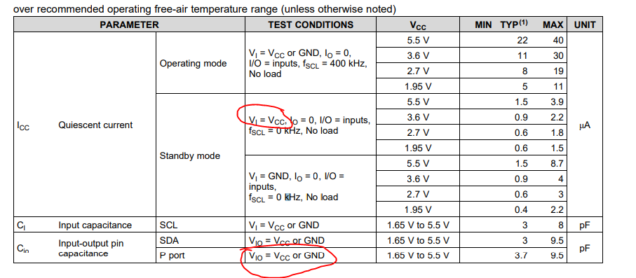
On the page 6 of TCA9535's datasheet,  for the test conditions of ICC standby mode:

1. what does VI stand for? VI=Vcc,  means that on the condition of when we set VCC=5.5V/3.6V/2.7V/1.95V listed in the table?

2. Io=0,  what is Io, which pins are the Io? or how to set Io=0?

3.I/O=inputs,  what does it mean? which pins are the I/O? what is the inputs?  how to set I/O=inputs?  

We want to test the ICC, but don't know how to set the test conditions correctly.

could you help explain it one by one ? 

  • our customer complain that the TCA9535 they recived recently consumes higher standby-current than the earlier version of LOT.No's devices, and the standby current is exceeds normal rank.

    so we want to know how to set the test conditions and verify whether the standby current is OK.

    Thanks a lot


  • Hi Jesse,

    Standby current is measured with all ports configured as inputs that are either pulled high (to VCC) or low (to GND) and the I2C port idle.  Does this match your test conditions?  What values are you seeing?  Do you think we could review a schematic so that we can better understand your application?

    Regards,
    Max

  • Thanks for your reply.

    But i don't think I can understand these conditons:

    1.VI=VCC??  what does it mean?

    2. Io=0?

    3. I/O=inputs,  I think this stands for what you said "all ports configured as inputs that are either pulled high (to VCC) or low (to GND)".  Am I right?

    our test conditions are:

    1. we mounted the TCA9535 only on our PCB board without any other IC or resistors/capacitors

    2. applied 3.3V on VCC and connected GND to ground.

    we test the abnormal values are around 2mA,  while the normal values are 460uA.

    please refer to schematic


  • I have marked the test conditions on page 6 of datasheet,

    I can not understand VI=Vcc, Io=0

  • Hi Jesse,

    "VI" is referring to the voltage at each IO port.  "IO" is referring to the output current from these ports.  Basically, the IOs are unloaded and configured to be inputs that are pulled high or low.

    Max

  • Hi Max 

    Thanks for your information.

    If "VI" is referring to the voltage at each IO port,  what is "VIO" referring to?  

  • It's the same thing.  For the VCC spec the ports are configured as inputs only, so the term VI is used.  For Cin the ports could be either inputs or outputs, so VIO is used.  I agree it could be clearer.

    Max

  • Thanks

    For VI=VCC, do we need add pull-up resistors on I/O ports?

    For SCL/SDA, can we left them float? because "At power on, P00 is configured as an input"

  • Jesse,

    Yes, you should use pull-up resistors on the IO ports in order to bias them to a high level.  (If they are biased to an intermediate level, supply current could be higher).  SCL/SDA should typically be pulled up as well, but you won't need to configure the device outside of the default state since the IOs default to inputs at power-on.

    Regards,
    Max