This thread has been locked.

If you have a related question, please click the "Ask a related question" button in the top right corner. The newly created question will be automatically linked to this question.

SN65176B: The value of A,Bpin's voltage when 0V was input to RE, DE, and D pins(Vcc=5V)

Part Number: SN65176B

Dear all,

I would like to ask the following questions.

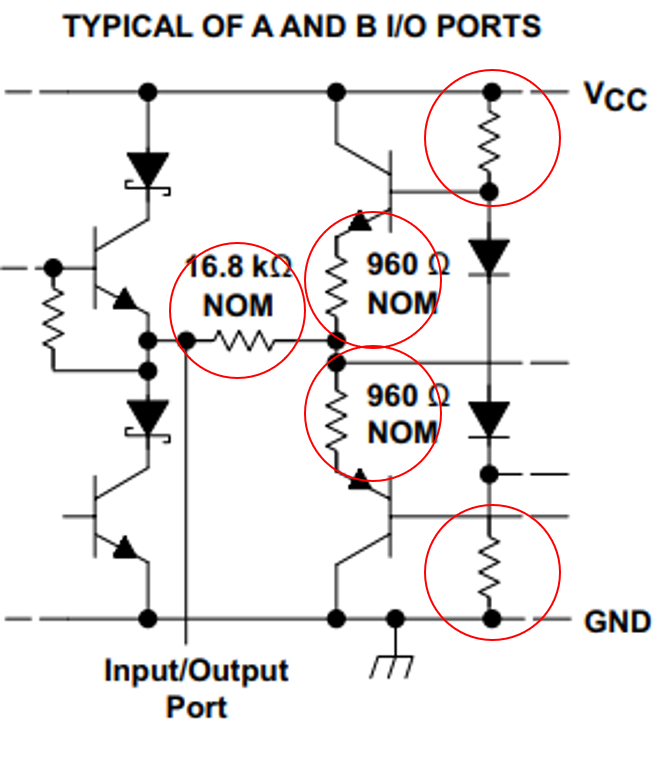
As shown below, when 0V was input to RE, DE, and D pins(Vcc=5V), the output of A and B was 1.4V. I want to answer the following questions

1. I think that the current of 58μA flows out from the A and B pins, and it flows to GND through the pull-down resistor, so that 1.4V is output.

The data sheet includes the following.

In this description, only the voltage input to the A and B pins is 12V and -7V, but how much current flows when the input voltage is 1.4V?

2. I heard from the customer that the voltage on pins A and B was measured under the same conditions as above, and that there was a difference of several commas.

I think that this phenomenon is because there is a difference in the current flowing out of A and B, is it correct?

Also, if there is a difference, how much current difference is there?

Best Regards,

Y.Ottey

  • Hello,

    Under this condition (device powered, driver disabled), the A/B pins will be weakly biased by the IC to about VCC/2.  You can reference Figure 19 in the datasheet to get a better understanding of the equivalent circuit.  For case #1 where there are weak external pull-down resistances, the output voltage would be expected to be between VCC/2 and GND.  In case #2 where the voltage is measured using a high-impedance measurement circuit like an Ohmmeter that sinks negligible current, the voltage would be higher.

    The bus input current specifications in the datasheet were taken at the extremes of the operating voltage range to show worst-case variation.  The I/V characteristic is dominated by the input resistance of the receiver, though, so the input current could be expected to vary linearly with voltage within this range.

    Please let me know if this is unclear or if you have any further questions.

    Regards,
    Max

  • Dear Max

    Thank you for your reply.

    I would like to ask additional questions about the second of my questions.

    The following circuit diagram is available in the data sheet p.19.

    1.Assuming that the Input / Output Port in this figure is an A or B pin, can I think that the A and B pins each have the following circuit inside the IC?

    2.Is it okay to recognize that the resistance indicated by the red circle is different between the A-pin side circuit and the B-pin circuit,

    and that this time there is a slight voltage difference between the A-pin and B-pin?

    3.Also, is the difference in resistance value recognized in order to create a voltage difference between the A and B pins?

    Regards,

    Y.Ottey

  • Yes, you can consider this structure as being present on pins A and B.  There may be minor differences in pull-up versus pull-down resistance values between the two pins, and these differences would create slight differential offsets.  If a fixed offset is needed, for example for "failsafe biasing" of the bus to a high level when undriven/open, then external pull-up/pull-down resistances could be used.  You can read more about failsafe biasing in this blog post:

    https://e2e.ti.com/blogs_/b/industrial_strength/archive/2016/12/06/rs-485-basics-two-ways-to-fail-safe-bias-your-network

    Regards,
    Max