This thread has been locked.

If you have a related question, please click the "Ask a related question" button in the top right corner. The newly created question will be automatically linked to this question.

P82B96: Inquiry for P82B986 specification

Part Number: P82B96
Other Parts Discussed in Thread: TCA9543A, PCA9306

Hello team,

I would like to use P82B96 as the following block diagram.

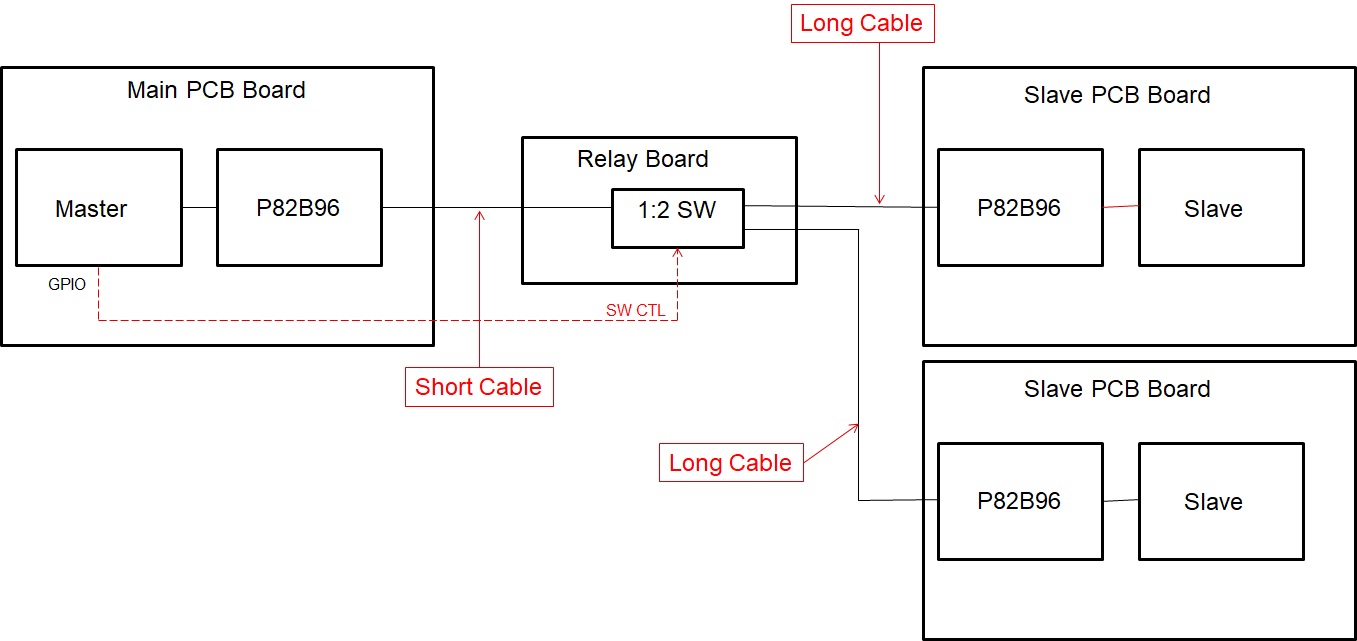
But I am concerned because I found the following in the datasheet. 

So I have some questions.
Q1) Can we use P82B96 as the above block diagram?
Q2) If Q1 is yes,  can you say  what switch IC is recomended? 

Your help would be so appreciated.

Best Regards,
Akihisa Tamazaki


  • Hi Akihisa,

    I do not see a problem with the P82B96 being used in the application shown above. The section you highlighted refers to the static-voltage-offset (SVO) used on the SCL (Sx) and SDA (Sy) side of the device. As long as two sides with SVO are not connected together, they will not interfere with each other. 

    I will be back in touch with switch recommendations. Are there any specific design requirements for the relay board?

    Regards,

    Eric

  • Hello Eric-san,

    Thank you for your prompt reply.

    I think that there are no specific requirement.  I would like to try I2C communication between Master and 2 x Slave which are switched by GPIO  of Master. Pull up of SDA and SCL lines is  5V. 

    Do you have a recommended  switch  IC?  I think that the low Ron device would be good.

    Best Regards,
    Akihisa Tamazaki

  • Hi Akihisa-san,

    Switch selection for this case is a bit tricky. Since the Tx/Ty side of the device has different threshold characteristics and driver-strengths than your typical I2C driver in order to support much larger bus capacitance, most traditional switch solutions will not be suitable for such an environment.

    In the case that the switch has enabled both slave lines and then needs to ACK back to the Master, it would need to drive the entire cable network worth of capacitance in the allowed time for the ACK. Because our switch devices are designed to work on a 400pF bus, this will likely not be possible.

    I would suggest using TCA9543A to switch the I2C bus prior to P82B96 on the Master board (this would require another P82B96 to drive the second line) and effectively have two Tx/Ty bus cables coming from the Main PCB. This would eliminate the need for the Relay Board, but still allow the switch to be controlled by the I2C master without any extra I/O pins.

    It would also be possible to switch the P82B96 Tx/Ty lines with a pass-fet buffer solution with an Enable feature such as PCA9306. However, this would require two buffer devices connected on the I2C bus in parallel to be controlled by I/O from the MCU to enable/disable to act as switches. Though the pass-FET nature of this device would likely be more suitable for the high-capacitance bus than a true-buffer, it is still not designed to operate in such an environment and may have some undesired behaviors.

    Let me know if you would like clarification on either of these suggestions or if there are any more design requirements you would like to take into account.

    Regards,
    Eric

  • Eric-san,

    Thank you for your comment. I see.
    If I have additional questions, I will post an another E2E thread.

    Best Regards,
    Akihisa Tamazaki