This thread has been locked.

If you have a related question, please click the "Ask a related question" button in the top right corner. The newly created question will be automatically linked to this question.

SN65DP141: Strange operation ?

Part Number: SN65DP141

Dear TI-er.

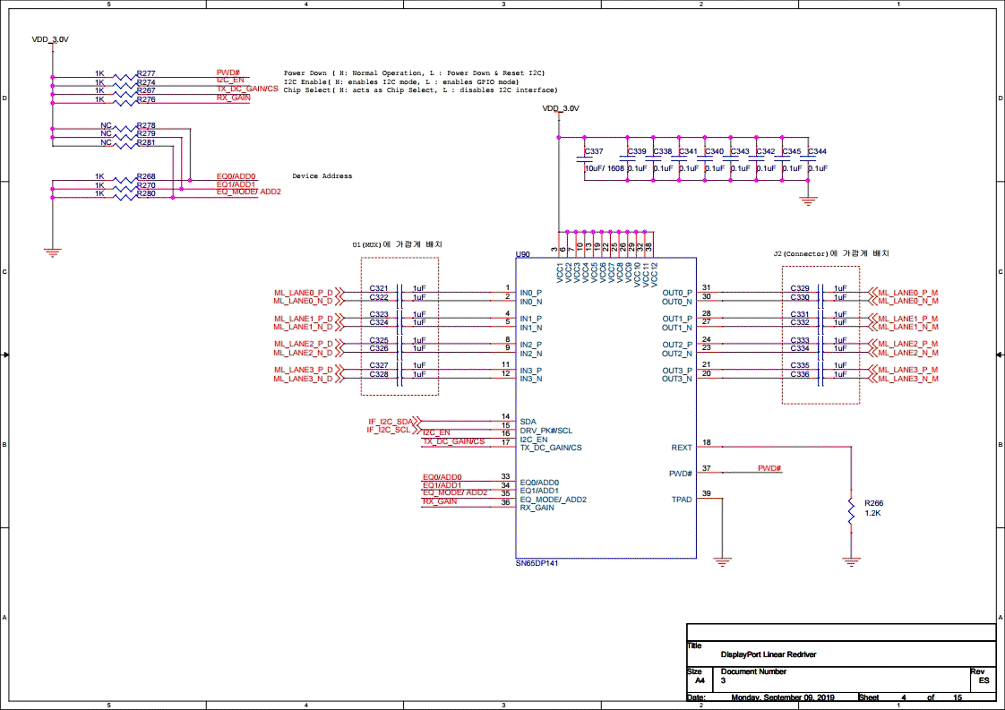
My customer is designed his board to SN65DP141.

1. He didn't control PWD#(Power down) in the board.

     after 1 minute, clearly good operation.

2. He control PWD#=high after 5seconds in power on state.

    It is good operation.

Do you know the strage operation ?

plz help me.

  • PWD# has an internal 200k pullup.

    How is PWD# being connected on the board? Would you please provide a scope capture of VCC and PWD# during power up?

    Thanks

    David

  • Hi, I'm the customer mentioned above.

    I will explain in detail agin.

    On current board, PWD# Pin has Pull-Up 1K with 3.3V and is always on.
    There is no control signal.
    VCC is also 3.3V and the voltage turns on as soon as power is applied.
    In this state, it takes a few minutes for the data received by the FPGA to stabilize.

    I connected the PWD # Pin with 1K Pull Down, modified it so that it could be controlled from the FPGA, and retested it.
    After 5 seconds of receiving normal DP signal(from PC), PWD# Pin was changed to High.
    That way, the FPGA immediately receives normal data without data settling time.

    If the delay is shorter or longer than 5 seconds, I will have other problems as well.

    Is there a sequence in SN65DP141 that I don't know about?

  • Please make sure DP141 comes out the power down after the VCC ramps up. Since there is an internal 200k pullup, there is no need to have the 1k external pullup. You do need a external capacitor to GND on the PWD# to provide the delay between the PWD# and the VCC. The capacitance depends on the ramp up time of the VCC.

    Thanks

    David

  • I understand about pull-up resistor that you told me.
    However, if PWD # is left in the default high state, it does not work normally, so There is no meaning.

    As mentioned above, I also know that a delay between VCC and PWD # High improves the phenomenon.
    There are two ways to deal with delays: using the CAPs mentioned or controlling them with the FPGA.

    The Pivotal Question is, is it appropriate to use this delay?

    Even if it works properly, you may have problems writing it if it is not used correctly.

    Thanks for the reply.

    Rhee.

  • Rhee

    To ensure the proper operation of DP141, please make sure DP141 comes out of the power down after the VCC has been stabilized. You can create this delay between the PWD# and VCC either passively or actively.

    The passive solution is to use the cap, and you can use RC time constant to calculate the required capacitance based on the VCC ramp up time.

    The active solution is to use the FPGA driving the PWD#. You want to make sure the FPGA is driving PWD# high after the VCC has been stabilized.

    Thanks

    David

  • The figure below is a graph with the gap between VDD and PWD # by adding a cap to the PWD # pin.
    (1K Pull-up and 1uF CAP applied, refer to data sheet circuit.)

    When the curve of PWD # reaches 90%, VCC is already stabilized, so it should be operated normally, but it is not.

    It operates normally only when the PWD # signal is changed to High 5 seconds after receiving DP Main Data.

  • Rhee

    Are you sending the DP main data before PWD# go high or after PWD# go high? Can I take a look at your schematic?

    Thanks

    David

  • In the initial circuit, since VCC was applied and PWD # became High, PC main data was transferred after PWD # High.
     ---> Strange Operation(After a few minutes, DP data received by the FPGA stabilizes.)

    Since then, the board has been modified to control the PWD # signal from the FPGA.
    The DP Main Data sent first and after 5 seconds the PWD # go to high.
    -> Normal operation

    The DP141 circuit configuration is shown below.

    Power is VCC_3.3V used collectively throughout the board.(Net name is 3.0V but Acually 3.3V)
    I2C is controlled by the FPGA.
    The other pins are not controlled.
    In the previous answer's graph is measured by adding CAP in this schematic.
    The basic circuit has the same ramp-up timing of VCC and PWD #.

    Thanks for the reply.

    Rhee.

  • Rhee

    Since I2C is controlled by FPGA, when do you program the DP141?

    Can you please dump out I2C registers of DP141?

    Thanks

    David

  • After powering on the board, I use the PC software to do an "Initialize" operation.
    This process is to set up the board settings
    "Initialize" is done by manually pressing the button on the software using the FPGA Register settings from the .ini file.

    The DP141's settings is proceed by this process.
    DP communication of HPD, AUX, etc. is also done during "Initailize" operation, and delay is set between HPD, AUX communication and DP141 setting through .ini file setting.

    Currently, the register of DP141 is setting only the captured part below.

    "Strange opreration" is apt to occur when the worst case condition that the video is output(that is, the gain setting is minimized.)
    It is difficult to say the exact value because the condition depends on DP cable, graphics card, etc.

    Usually set to a value of about 00110111.

    RSVD: 0 is Fix
    TX Gain is usually set to 0.

    Thanks for the reply.

    Rhee

  • Rhee

    What does ML_LANE[n]_P/N connected?

    Besides programming Channel 1, are you also programming Channel 0, 2, and 3?

    I would expect the sequence to be VCC -> PWD -> DP141 and FPGA configuration -> HPD going high -> AUX link training, is this the sequence you are following?

    Thanks

    David

  • #ML_LANE [n] _P / N is also connected to the FPGA(GTX Bank) and all four lanes are programmed.

    The current sequence is as you say.
    Unmodified boards will have both VCC and PWD# virtually high at the same time.

    Thanks.

    Rhee.

  • Rhee

    So #ML_LANE [n] _P / N_M is connected to the FPGA? 

    Can you please show a scope capture of VCC, PWD# and HPD?

    Does FPGA make sure the DP141 is fully programmed before driving HPD high?

    Thanks

    David

  • ML_LANE [n] _P / N_D is Data coming from Source
    ML_LANE [n] _P / N_M is connected to the FPGA.

    In short, the structure is Source-> Connector-> DP141-> FPGA.

    As mentioned in the previous answer, HDP does not work unless I manually run the software.
    VCC and PWD # rise immediately when only power is applied to the board.

    Since it is a manual operation method, it is meaningless to check the timing with Scope.

    The graphs of VCC and PWD # are in the previous answer.
    In case you don't know, only HDP is taken separately.

  • Rhee

    You probably don't need the AC coupling caps on the ML_LANE [n] _P / N_D since the AC coupling caps should already be present on the SOURCE side. Having AC coupling cap in the SOURCE and on the input of DP141 would reduce total capacitance, possibly fail the DP spec AC coupling cap requirement.

    I am looking at this problem from a system configuration and a signal integrity perspective. 

    From a system configuration perspective, I would expect expect the sequence to be VCC -> PWD -> DP141 and FPGA configuration -> HPD going high -> AUX link training.

    From a signal integrity perspective, do the SOURCE or FPGA have any registers indicating the link training status? Between the two cases you reported, does the link training end up with the same result? Do you see a difference in time when you use a short or a long cable between the source and the DP141?

    Thanks

    David

  • Stabilization times vary slightly in the same environment, making it difficult to tell for sure.

    However, as mentioned above, this phenomenon is most pronounced under worst-case conditions (minimizing the EQ setting of the DP141).
    The worst condition depends on the length and condition of the cable.

    In FPGA, there is a way to check the signal status.
    It seems difficult to verify at Source.

    Thanks.

    Rhee.

  • Rhee

    Depends on the FPGA RX design capability, any ISI not compensated by the EQ of DP141 will have to be handled by the FPGA RX. 

    The phenomenon could also depend on how the FPGA core handle the link training, whether it goes through multiple iteration of different DP data rate and lane count. Hopefully this can also be printed out by the FPGA.

    Thanks

    David

  • We already know where data compensation is possible in an FPGA.

    However, if the source and FPGA are connected directly without DP141, there is no issue of settling time.

    Once stabilized, additional compensation can be made with the FPGA, but the previous situation is a problem.

    Has there been no sequence or other issues with this before?

    Thanks.

    Rhee

  • Rhee

    Have you tried to replace the AC coupling caps on the input with 0 ohm resistor? 

    I have not seen this issue in the past. Once PWD# is driven high after VCC is stabilized, and with both FPGA and DP141 properly programmed, the system should be in proper operation.

    Thanks

    David