This thread has been locked.

If you have a related question, please click the "Ask a related question" button in the top right corner. The newly created question will be automatically linked to this question.

TCA9406: falling edge of SDA_A and SCL_A is not monotonically decreasing

Part Number: TCA9406

Hi there,

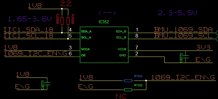
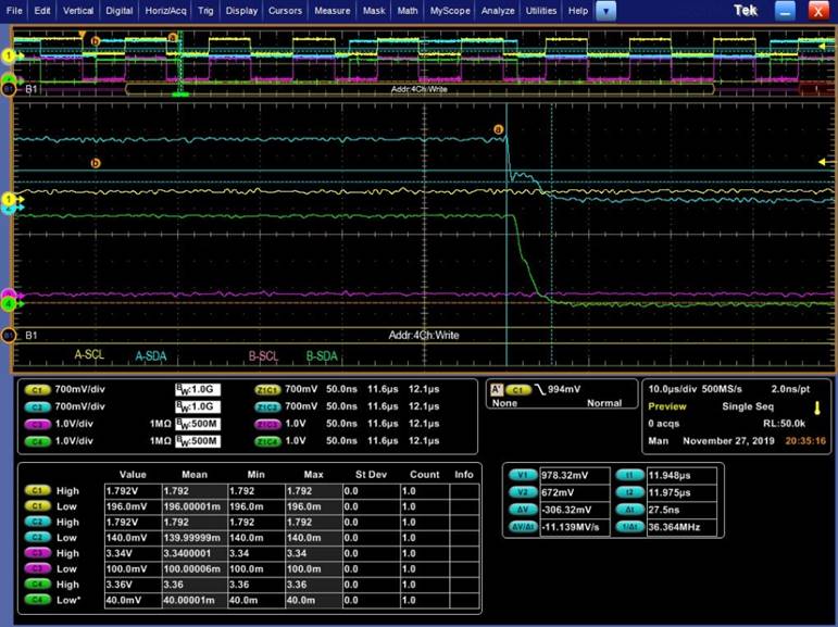
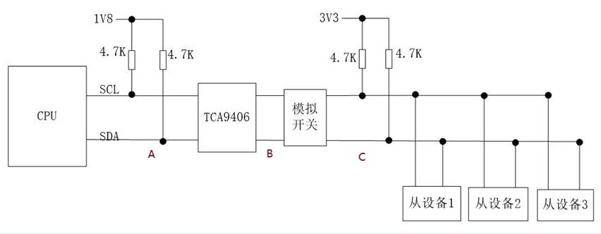
My customer found the falling edge of SDA_A and SCL_A is not monotonically decreasing. The glitch may trigger data error of I2C communication. After disconnect SDA_A and SCL_A from I2C bus, the glitch disappears. Customer replaced TCA9406 with TCA9417, and it doesn't have the same issue.

My question is how to eliminate the glitch of TCA9406.

Thanks.

  • Hi Jerry,

    The small spike you're seeing is caused by the pass-FET of TCA9406 turning on. If the A-side is pulling low, this would be the point where side A and side B become connected. Because side B has some capacitance on its bus, it discharges through the FET and slightly charges the A-side bus. This is a product of the pass-FET architecture whereas other True Buffer solutions re-drive the signal and do not experience this discharge. 

    This small glitch should not cause any data errors. The I2C standard specifies a deglitch filter to ignore any pulses 50ns or less. Since the glitch you're seeing appears to be less than 20ns, this will not be an issue. 

    Let me know if you have any more questions. 

    Regards,

    Eric

  • Hi Eric,

    In another project, the glitch is about 40ns. Is there any way to reduce it?

    Thanks.

  • Hi Jerry,

    Does the other pulse look similar in magnitude and shape? This is likely due to a higher secondary bus capacitance in the other project. In this case, more charge would have to dissipate to the other side when the FET activates. Because this spike is partially caused by the difference in capacitances of each bus, making the two sides more similar would likely decrease the severity of this spike. Reducing secondary bus capacitance is likely preferable to artificially adding capacitance to the primary bus.

    Are you probes connected close to the driving device or close to PCA9406 in your measurements? The spike is likely more attenuated further from the connecting FET. If the driving device is at the end of the I2C line, it would take advantage of the full trance parasitic capacitance to attenuate the spike from the two buses connecting. 

    Also note that this spike will only occur on the driving side of PCA9406. If the driving device and receiving device are not on the same side of PCA9406 then the driver will likely ignore this artifact. Also note that this glitch would not effect data because these transitions would happen during a constant clock state. Data is read on clock edges so extra data edges will not effect data. I understand this could potentially impact clock signals. 

    If this is a concern and you can share your schematic, I can point out possible ways to mitigate the potential impacts of this phenomenon.

    Regards,

    Eric

  • Hi Eric,

    I totally understand the first two points. For the last point, I don't understand what 'same side' means. I attach the waveform, block diagram and schematics. Yes, they have a 1:3 analog switch at the B side of TCA9406, which would introduce more parasitic capacitance. The cared points in below figures are Waveform A, Point A and  SCL_A/SDA_A.

    I'm on business trip. You could suggest what I could have a try to reduce the glitch or to verify it wouldn't affect the I2C communication. I will go to customer side for on-site demonstration after coming back.

    Thanks.

  • Hi Jerry,

    Thanks for the scope shots. They help clearly show how the spike on the A-side occurs when the voltage on the B-side begins to fall. 

    I will try to give an example of what I mean by "same side" given your layout diagram:

    The CPU Master device is on side A of TCA9406 and all slaves are on side B. This means that there will never be a case where communication will occur between two device that both exist on the same side (both A-side or both B-side) of the bus. Because the spike only occurs on the driving side of TCA9406 (appears on blue probe and not green) this should not cause communication problems for the receiving device. 

    If you would like to dampen this spike, small series resistance on the B-side near TCA9406 would limit the rate that the B-side will discharge. This will add to the effective Vol seen by B-side slaves. 

    Let me know how your demonstration goes and if you would like any more information beforehand.

    Regards,

    Eric