This thread has been locked.

If you have a related question, please click the "Ask a related question" button in the top right corner. The newly created question will be automatically linked to this question.

DS250DF410: write global register 0xFF failed

Part Number: DS250DF410

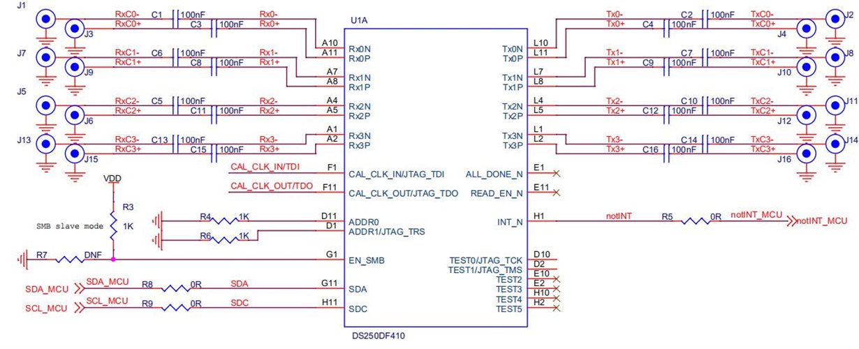
Hi, I'm using DS250DF410 retimer now, the schematics of IO signals attached. the I2C controller is STM32 mcu, the current issue are:

1. there is 25MHz clk supplied at pin Cal_Clk_In, but the Cal_Clk_Out Pin is 2.5V DC signal when power up, I don't know it's correct or not;

2. I could read global register and got device ID is 0x0E, version ID is 0x31 and device ID is 0x10, that means register read operation should work, but the register 0xFF read value is 0x00, I don't know this default value is correct or not;

3. I tried to write the 0xFF register, i.e., 0x01 to enable channel, but the read back value is still 0x00, I tried write other RW registers, all results shows write operation failed, I cannot change the default value, but from the scope, I saw there is ACK after the write byte operation. is there any other process needed before write register?

thanks in advance!

  • Hi,

    I will review and provide my suggestions by close of business tomorrow, Wednesday USA Pacific Time.

    Regards,

    Rodrigo Natal

    HSSC Applications Engineer

  • Hi,

    Your retimer schematic looks correct for operation in Slave Mode. I'm assuming that R7 is not populated (it should NOT be.)

     Some questions below:

    1. Can you confirm you are using correct two-wire serial addressing and data protocol
      • For your case both ADDR0 and ADDR1 have 1kOhm to GND, thus specifying 0x30 as the retimer 8-bit address. This is the address you should be using for operations. I'm assuming there is no other device on the bus with this same address
      • Note that some software I2C programs utilize a 7-bit addressing format for operations. If that is your case you would need to adjust 0x30 address value for 7-bit addressing
    2. Are you using the register operation format as per the example below for selecting a channel?


    REG       Value     Mask       Comment

    FF          01           FD           //Enable Channel Access and Disable Share Access

    FC         01            FF           //Enable Register Access to Channel 0 of Die 0

    Cordially,

    Rodrigo Natal

  • Hi Rodrigo,

    thanks for reply. 

    1. Yes, R7 is not populated, DNF means Do Not Fit;

    2. no other device on SM Bus, only one MCU as controller and one DS250DF410 as slave, I could read device ID, that means BUS communication should be OK;

    3. Yes, we know the I2C 7bits addressing method, we set the read/write bit at the lowest address bit;

    4. we tried to write 0xFF register by below configuration:

    REG       Value     Mask       Comment

    FF          01           01           //Enable Channel Access and Disable Share Access

    I also tried the configuration you mentioned using mask 0xFD, the writing operation still failed.


    In other hand, I'm worried a little about whether my chip is broken or not. Below question may also need your help:

    1. What's the default signal at CAL_CLK_OUT pin, we observed 2.5V DC signal;

    2. I checked the board total power is 500mW, considering 93% efficiency of TI DC/DC chip, and then minus about 100mW of STM32, I roughlly guess DS250DF410 consumpt about 365mW when power up, is it a reasonable value?


    thanks.

    hainan bai

  • Hi,

    1. CAL_CLK_OUT should be a buffered replica of CAL_CLK_IN.
    2. The typical static power consumption value (i.e. for no high-speed data present at channel inputs) is 329mW. Your figure is not far from that

    Cordially,

    Rodrigo Natal

    HSSC Applications Engineer

  • Hi Rodrigo,

    thanks, I checked the CAL_CLK_IN, there is 25MHz input, but there is 2.5V DC signal at CAL_CLK_OUT pin, does that mean my chip is broken? oh no. Do you have any other suggestion to save the chip? thanks.

  • Hi,

    Please follow the link below for submitting a device return request to enable TI analysis.

    http://www.ti.com/support-quality/additional-information/customer-returns.html

    Regards,

    Rodrigo Natal