


Hi All,
I have an application in which I am using this IC to convert LVDS differential signals to single-ended signals and then use it with FPGA.
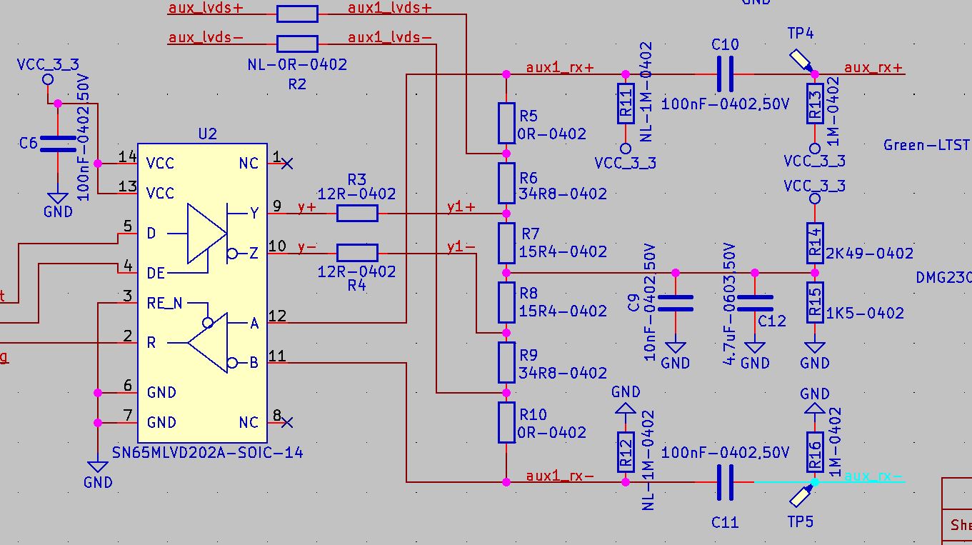
I have been provided with the above reference circuit and I am not able to understand the termination network here. Please find below points.
For the receiver section, it's easy to understand that the aux line has 100ohm differential impedance and its terminated by Split termination technique with the help of R6, R7, R8, R9,
that combination of resistor makes it 2 x (34.8 ohm + 15.4 ohm) = 100.4ohm which is near to 100ohm and that's ok.
(1)For the Driver section why its terminated with help of R3, R4 first(which seems like source termination) and then split terminated with help of R7 and R8?
here its 2 x 15.4 ohm = 30.8 ohm. I especially don't understand this part of the termination.
(3)Can this IC directly support 100ohm differential lines?
(4)Can we simplify this complex termination network?

