This thread has been locked.

If you have a related question, please click the "Ask a related question" button in the top right corner. The newly created question will be automatically linked to this question.

TPD6S300A: Will leakage occur when OVP event is triggered?

Part Number: TPD6S300A
Other Parts Discussed in Thread: TPD6S300, TPS65987D

Hello expert,

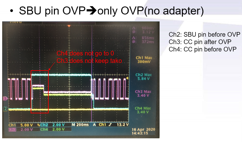
Customer would like to double check if there is leakage from CC1 to C_CC1 through body diode when OVP event is triggered. Could you kindly help to double check? Thanks a lot! 

Best regards,

Ann Lien

  • Hello expert,

    Add waveform here. We did SBU OVP test with 5V level and found out CC will be triggered to a uncertain level. We don't understand why the behavior is like that. That's why we are wondering if there is any leakage here and it seems like CC FET is not disconnected totally. Thanks a lot!

    after OVP/before OVP = after TPD6S300A/before TPD6S300A.

    Best regards,

    Ann Lien

  • Hello Ann,

    Which pins are you applying the OVP event to? C_CC1 or CC1?

    The C_CC1 pin would be connected to the Type-C connector on your system, which is what the TPD6S300A is designed to protect an OVP event from.

  • Hello Adam,

    They tested SBU pin and it seems like CC pin will be influenced to a uncertain level. We are wondering if there is any leakage on it. Thanks!

    Best regards,

    Ann Lien

  • Hi Ann,

    Which SBU pin was the over voltage event presented on? C_SBU or SBU? Also, was there a constant voltage applied to Vpwr pin throughout the tests?

  • Hello Adam,

    We tested on C_SBU, close to connector side, as ch2 in waveform. And we tested with constant 5V on power supply. Customer is waiting for reply and they test competitor part, it seems like normal behavior. please kindly help. Thanks!

    Best regards,

    Ann Lien

  • Hi Ann,

    Thank you for the clarification. Looking at the original scope captures you shared, they are difficult to follow as I am not sure what you mean by before and after OVP. Would you be able to conduct the tests again, but label the relevant channels based on their pin names (C_SBU1, SBU1, C_CC1, CC1).

    Also, as you conduct your tests, please follow the testing guidelines as described in the following document. This is for the TPD6S300, but the design is very similar so the test procedure is the same

    http://www.ti.com/lit/ug/slvuax4/slvuax4.pdf

  • Hello Adam, 

    after OVP --> system side

    before OVP --> connector side

    For waveform 1,

    Ch2 -->C_SBU1

    Ch3 -->CC1

    Ch4 -->C_CC1

    For waveform 2,

    Ch1 -->connector side VBUS

    May I know if it is okay to judge? It seems like CC pin is influenced by SBU OVP event. Thanks!

    Best regards,

    Ann Lien

  • Hi Ann,

    I replied to Oliver in the email but I will reply to this thread as well. The waveforms you are seeing are expected since you are evaluating the TPD6S300A on the TPS65987DEVM. There is no leakage current through the protection device, and the voltage pullups you are seeing on the CC channel is from the TPS65987D presenting an Rp after the disconnect.