This thread has been locked.

If you have a related question, please click the "Ask a related question" button in the top right corner. The newly created question will be automatically linked to this question.

DP83867IR: Compliance test(A and B peak voltage) fails

Part Number: DP83867IR

I am working on a custom board with three DP83867IR parts on it, using the Pulse HX5008NL magnetics and a Stewart SS-7488S-YG-PG4-BA RJ45 connector. It is currently failing the 1000base-T Peak Voltage tests for points A and B - the peaks measure at about 565mV (the minimum required is 670mV) on all three channels. The mask tests all seem to pass. The layout guidelines in the data sheet have been followed as closely as possible. I've searched through the E2E boards for answers, but didn't find anything definitive. The PHY is outputting the proper mode-1 waveform with the same peak voltages on all 4 pairs. Any insights you can provide will be appreciated.

  • Hi John,

    We have a app note to explain the register settings needed for compliance testing: http://www.ti.com/lit/an/snla239a/snla239a.pdf

    Can you check that these register settings are used?

    -Regards

    Aniruddha

  • Hi Aniruddha,

    That is the app note I used to determine the register settings for my test. At first I was only seeing the mode 1 waveform on the 'A' pair, but I found a reference that register 0x0025 is in the extended address register range, so modified my settings to account for that and am now seeing the waveform on all four pairs.  Here are the register settings I am currently using:

    reg 0x001F 0x8000
    reg 0x0000 0x0140
    reg 0x0010 0x5008
    reg 0x0009 0x3B00
    reg 0x000D 0x001F
    reg 0x000E 0x0025
    reg 0x000D 0x401F
    reg 0x000E 0x0480

    I also read that setting the 0x01D5 register is only necessary on the 48-pin version of the part - is that correct?

    Best regards,

    John

  • Hi Aniruddha,

    Do you have any further suggestions?

    Thanks,

    John

  • Hi John.

    Thanks for your patience on this, the register settings that you showed are correct. Yes, 0x01D5 is applicable to 48pin version. Are you using 64 pin version? Can you possibly share your schematics, we can use E2E private chat if posting here is not possible for you?

    Another thing that I would like to confirm is that you are using small cat5e cable (<2 inch) when performing the compliance measurement. Also the total distance from the PHY to RJ-45 connector on the board should not be too long and is typically in the order for 3-5 inches. Longer traces or any interconnects (like board connectors) can cause the voltage to drop. This doesn't necessarily mean that the system has any problems, its just that the signal will naturally decrease and the measurement will need to be done as close to the device as possible.

    -Regards

    Aniruddha

  • Hi Aniruddha,

    I have attempted to share two schematic pages in pdf format here (I can see a placeholder - please let me know if you can see the contents)

    The cat5e cable I am using is the one that came with the compliance test fixture from Tektronix.  The overall tip-to-tip length is 4", the spacing between the connector shrouds is 1".  The overall distance from the PHY to the connector is approximately 1.2"

    Ethernet1 & 2.pdf

    Best regards,

    John

  • Hi John,

    In your schematics, the traces after magnetics have differential coupling symbol but the traces between PHY and magnetics do not have that symbol. Are they differential too? Can you check on that R545, R538, R528, R519 are not populated on the test board? Please also check that R139 (RBIAS) is 1% tolerance resistor.

    I also see that there are extra traces going to M12 connector. In this scenario, the traces and M12 connector will add extra parasitic on to the signal when you are trying to perform measurements from the J13 port. This can cause degradation of the signal.

    -Regards

    Aniruddha

  • Hi Aniruddha,

    The traces between the PHY and magnetics are differential as well, although it’s not indicated on the schematic itself.  R545, R538, R528 and R519 are all not populated, and R139 is a 1% 11k resistor.

    The M12 connector is in-line between the magnetics and the J13 port and is surface-mounted, so if it’s not populated (as in this case) there is no additional stub.  If and when we use M12, J13 will not be populated and there will indeed by stubs as a result – we are looking into ways to eliminate this dual-connector option in the future.


    I appreciate your insights and assistance in troubleshooting this issue.


    Best regards,


    John

  • Hi John,

    I would also recommend double checking the voltage at the supply pins and making sure that they are withing the datasheet spec. The component you have selected are correct so drop in VOD is not expected. Also check the voltage across RBIAS, it should be ~1V. Removing the dual connector option should also help reduce any signal loss. 

    -Regards

    Aniruddha

  • Hi Aniruddha,

    Here are the voltages measured (names are from the schematic):

    1V1_ENET:   1.096V

    2V5_UTIL:    2.425V

    1V8_ENET:   1.811

    RBIAS Voltage:  1.001V

    All of which are within the limits in the datasheet.

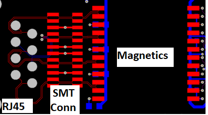
    Removing the dual connector option will have to wait for a board spin, but the SMT connector is not currently installed, so the differential pairs run from the magnetics through the SMT footprint to the RJ45 as shown below, with no stubs.

    Best regards,

    John

  • Hi John,

    The measured voltages you shared above look correct and the layout also looks as per recommendation. Just to clarify, are you planning on re-spinning the board and test it again? While the board get re-spinned, is it possible to test with more devices to see if they shows the same low voltage?

    I also took a look at some internal registers which can affect the output voltage. These registers are set to a default value which allows the PHY to be IEEE compliant and are not advertised in the datasheet for customer use. However in this case, can you read registers 0x9F, 0xA0, 0xA1? These are coarse and fine gain control registers for output voltage.

    From a logistics front, did you get the units recently from ti.com or are these older units? I want to eliminate the possibility that these are pre-production units.

    -Regards

    Aniruddha

  • Hi Aniruddha,

    I am glad to hear that the design and implementation look correct.  We are going to spin the board, but it's to a pre-production version and we really need to have it in the final configuration, so not a lot of opportunity for experimentation.  I can certainly hack on the existing boards if you've got some suggestions, or there is a possibility that I could argue for a very small test run.

    The register readings are:

    0x9f:    0x00

    0xA0:   0x1140

    0xA1:   0x7949

    These parts were purchased either late last year or early this year.  The marking on the components (I checked several) is:  91ACLFWG4, which I assume has a date code buried in it.

    I'm looking forward to your suggestions,

    John

  • Hi Aniruddha,

    I spent a little more time examining the registers this morning - as I said earlier there are 3 identical PHYs on the board.  I used the same set of register writes for each one to put them into Mode 1 (and verified that they all were in Mode 1 with an oscilloscope), but the readings from the three registers are not the same across the 3 PHYs.

    The register readings are:

                 PHY1           PHY2          PHY3

    0x9f:     0x00             0x00           0x00

    0xA0:   0xFFFF        0x140         0xFFFF

    0xA1:   0xFFFF        0x7949      0xFFFF

    As a sanity check, I verified that I could read back the values that I wrote to set Mode 1, and all three PHYs read back as expected, so it's not a communication issue.  The amplitude of the Mode 1 waveform peaks is essentially identical across the three PHYs as well.

    Best regards,

    John

  • Hi John,

    It looks like extended register access method is not being used on your software. Registers higher than 0x1F fall in the extended register space of the PHY and cannot be accessed directly. They have to be access indirectly as per the method mentioned in the datasheet section 'Extended Address Space Access'. Can you modify your register access method and try reading those registers again?

    -Regards

    Aniruddha

  • Hi Aniruddha,

    My bad - I should have remembered about indirect addressing for the extended registers.  I read the three registers for all three PHY's, using indirect addressing, the results were not identical:

                      Reg 0x9F      Reg 0xA0       Reg 0xA1

    PHY1:       0xBBBB          0x0001           0x0807

    PHY2:       0xBBBB          0x090C          0x0A0A

    PHY3:       0xBBBB          0x0706           0x0808

    I am a little surprised that the results are different between the PHY's, which makes me question my methodology.  Just as a sanity check, here is an example of the register writes I executed to access register 0x009F:

    mdio write ethernet@ff0b0000 0x000D   0x001F

    mdio write ethernet@ff0b0000 0x000E   0x009F

    mdio write ethernet@ff0b0000 0x000D   0x401F

    mdio read ethernet@ff0b0000 0x000E  

    The syntax is 'command' 'target address' 'register address' data

    Please let me know if I've made an error.

    Best regards,

    John

  • Hi John,

    It is possible for A0 and A1 to be different between different devices. They are for fine gain adjustment and are tuned to give out standard output voltage from the PHY. 9F is coarse gain adjustment and should be same for all devices. Your register access method is correct.

    I also received email from the TI FAE handling the account, which prompted me to take another look at the schematics. I notice that RXD2 and RXD0 lines are pulled to 1.1V. IO lines should be pulled to IO voltage which is 1.8V in your case. Is it possible to disconnect them from 1.1V and connect them to 1.8V?

    TX_D[7:4] are pulled to ground via 1kohm resistors and RX_D2/0 are pulled up using 1kohm resistors. Can you change all 1k resistors to 2.49k? 1k might be too strong and we have not characterized the device using 1kohm resistor.

    -Regards

    Aniruddha

  • Hi Aniruddha,

    I replaced all of the 1k resistors with 2.43k (the closest I have to 2.49k available in my kit at the moment) and moved the pullups to 1.8V as you suggested.  There was no change in the peak voltage levels of the compliance test.

    Is it possible to adjust the gain levels by writing to the registers you mentioned?  If so, what are valid ranges?

    Best regards,

    John

  • Hi Aniruddha,

    It was good to talk with you the other day.  I had a chance to take some measurements yesterday of both magnetic variants while I adjusted the value of register 9F:

                                 ETH0                         ETH1 

      (Wurth 749020010A)    (Pulse HX5008)

    9F Value           Point A                          Point A

    BBBB               580.71                        570.37

    CCCC              578.31                        570.62

    DDDD              577.47                        570.38

    EEEE              577.21                        570.19

    FFFF               576.97                        570.35

    In each case I read back the value of register 9F to ensure that it was set as I intended, but the peak voltage as reported by the compliance test application didn't seem to track.  I'm not sure exactly why that would be.  My oscilloscope is out for calibration (and I will be out of the office for a few days), but I should be able to repeat this test late next week.  In the meantime, do you have any idea why increasing the coarse gain would not affect the output?

    Best regards,

    John

                                ETH0                                       ETH1
                 (Wurth 749020010A)             (Pulse HX5008 magnetic)
     
    9F Value          Point A                                    Point A
    BBBB                580.71                                    570.37
    CCCC                578.31                                    570.62
    DDDD              577.47                                    570.38
    EEEE                577.21                                    570.19
    FFFF                 576.97                                    570.35

  • Hi John,

    This is very unusual. The coarse gain setting should have increase the output voltage. When you get your scope back, can you check the same test with the TI EVM? I have forwarded all the details to Errol but we can have a follow up discussion if you need help setting up the EVM.

    -Regards

    Aniruddha

  • Hi Aniruddha,

    I thought so too.  I've got the EVM in hand, and my scope just came back - once I get the EVM up and running I'll do the same test with it and post the results.

    Best regards,

    John

  • Hi Aniruddha,

    I got the EVM up and running, and repeated the test on it.  The results were:

                                EVM                        
     
    9F Value         Point A (mV)  
    BBBB                 746         
    CCCC                886       
    DDDD               1042      
    EEEE                1193          
    FFFF                 1299 
    I also repeated the test on my board and had the same results as before - basically no change in amplitude.  I'm pretty sure that I'm writing the registers properly on my board - I can set it to any of the test modes, and when I read back the value I write to register 9F, it is consistent.  So I'm not sure what's going on.
    I did run the 1000base-T compliance test on the EVM and it passes all of the tests, which helps to validate that the test setup is functioning properly.
    Do you have any idea why changing the value of register 9F doesn't result in a change in amplitude?  I duplicated this behavior on all three channels.
    Best regards,
    John
  • Hi John,

    Would it be possible for you to remove the PHY from the EVM and mount it on to your board and test your board again? The fact that you see registers change on your board tells me that your register access method is correct. However, it unusual that none of the channel show any change in output voltage after the register has been edited. 

    -Regards

    Aniruddha

  • Hi Aniruddha,

    That's a good notion.  I don't have the proper equipment to do the solder work at home, so I'll have to arrange a time to get into the office to use the equipment there.  Before I do that, I think I will use the launchpad board to drive MDIO/MDC on my board (I will lift the pins and solder in some jumpers), just to make sure that it's not a communications issue from my end.  After that I will see if we can swap the parts - possibly late this week.

    Thanks,

    John

  • Hi John,

    That also is a good check, let me know what you find from both the experiments.

    -Regards

    Aniruddha

  • Hi Aniruddha,

    Just an update - I was able to get into the lab to swap the parts, but neither one is currently funcitonal, so I need to go back into the lab to re-inspect my work.  I've also ordered some new parts just in case the parts got damaged during the remove/replace process.

    I also tried to drive the MDIO/MDC interface on one of my boards from the launchpad board with no success - I'm not sure what's going on there, but will continue to work on it. 

    I hope to have something more concrete for you later this week or early next week.

    Best regards,

    John

  • Hi Aniruddha,

    Finally, some good news!  I was able to remove and reflow the parts on both boards - the issue was that the ground pad had not reflowed, so there was no ground connection.  Here are my findings:

    • The evaluation board (with my original part on it) now fails the peak voltage test at 574.797mV.
    • Writing FFFF to register 9F on the evaluation board didn't change the voltage much - 575.442mV
    • On my board (with the original eval board part on it) now passes the peak voltage test at 706.289mV
    • Writing FFFF to register 9F changes the voltage substantially - 850.47mV
    • I ran the entire test suite on this channel, and everything passes

    The conclusion that can be drawn is that the original parts on my boards are not fully functional.  All of the boards I have tested through 2 prototype runs (a total of about 80 board, with 3 PHYs each - of which I have tested roughly 20) have the same lot code on all of the parts and have behaved in the same way.  The lot code for the parts on these boards is 9IACLFWG4 (note that the I may in fact be a 1 - it is hard to tell).

    The lot code on the original eval board part is:  83APKQWG4

    I also purchased some spare parts (in case the original parts got damaged during the remove/replace process).  The lot code on these parts is:  88AEL1WG4 (again, the 1 may be an I).  I will get some of these installed as soon as I can to evaluate them.

    It looks like we've found the root cause.  Thanks for the suggestion to swap the parts between boards - the results seem conclusive.

    Best regards,

    John

  • Hi John,

    Thanks for sharing the update and I'm glad that the issue was root-caused. If it's ok, I will close this thread for now. If you still run into issues after your next steps, you can post a new thread and link it to this one to provide context.

    -Regards

    Aniruddha 

  • Hi Aniruddha,

    Thank you for all your help.

    Best regards,

    John