This thread has been locked.

If you have a related question, please click the "Ask a related question" button in the top right corner. The newly created question will be automatically linked to this question.

DS90UB948-Q1: power over STQ

Part Number: DS90UB948-Q1
Other Parts Discussed in Thread: DS90UB949A-Q1, DS90UB914A-CXEVM, DS90UB913A-CXEVM, TIDA-020003, DS90UB949-Q1

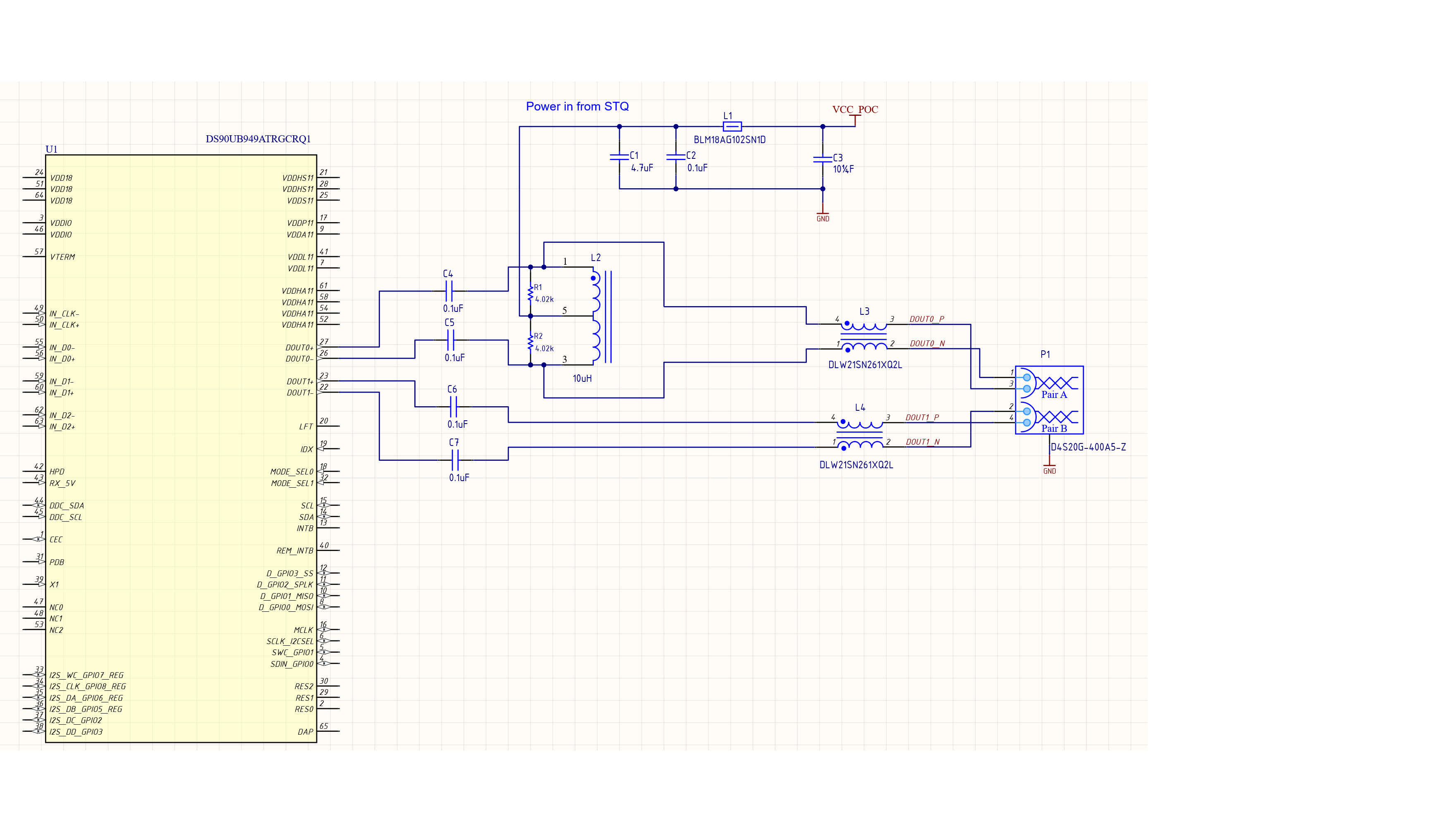
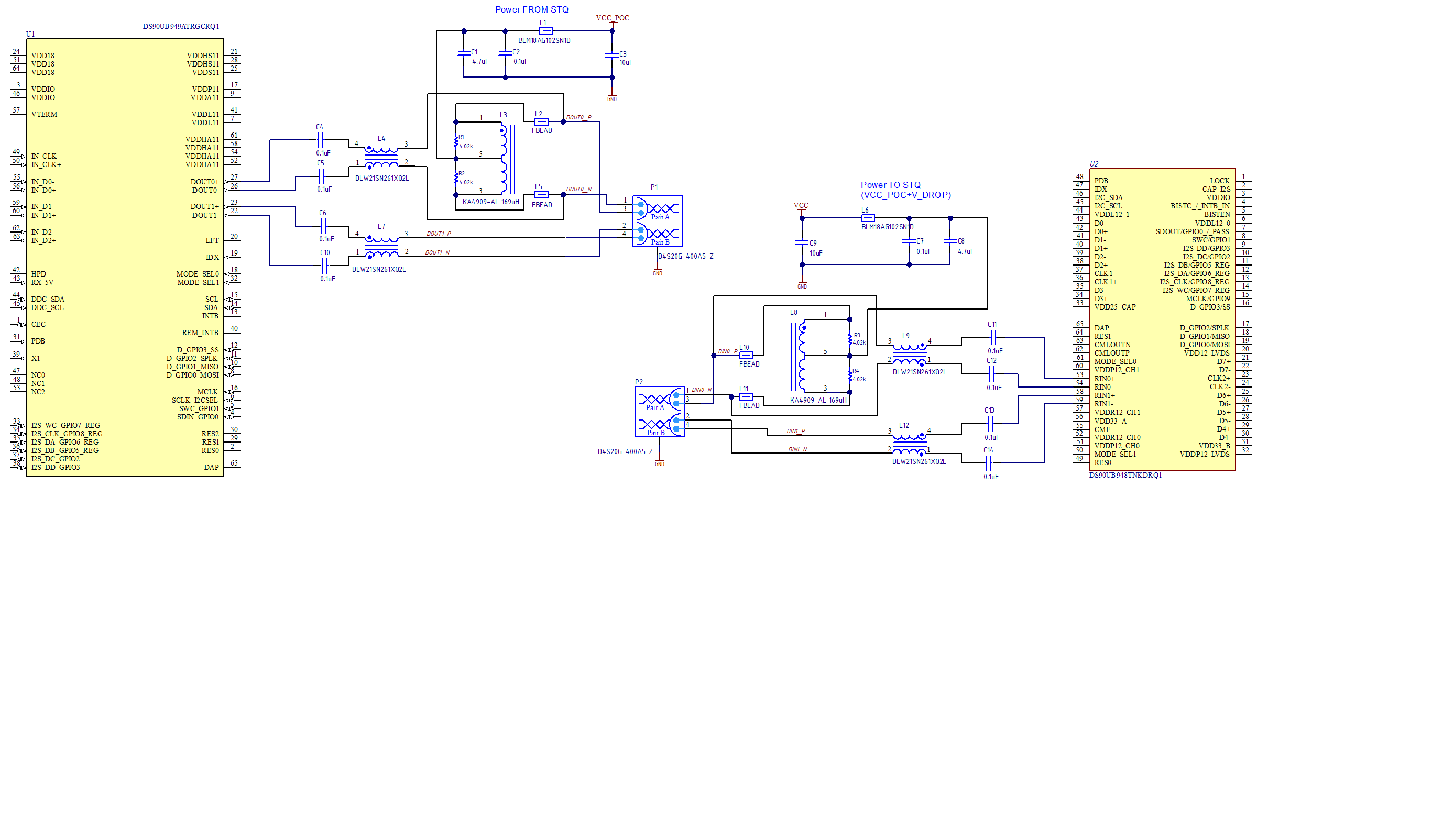
We're going to use DS90UB949A-Q1 and DS90UB948-Q1 pair in dual link mode with STQ cable (6 meters) for PCLK up to 192MHz.

It's desirable to implement power over cable.

I have following questions:

1. Is it possible to use concept of power over STP described in DS90UB913A-CXEVM & DS90UB914A-CXEVM evaluation modules in case of dual link over STQ for DS90UB949A-Q1 and DS90UB948-Q1 pair?

If yes,  should power be translated over each twisted pair inside STQ? or just one?

2. If i.1 is not working solution, can I switch to dual link with 2 coax and PoC?

Thank you. 

  • Similar concept as Power-over-coax can be used to couple power to STP or STQ. Same twisted pair (the pair that carries the data) can be used as shown above

    You can find more details and info in this EE times article done by the FPD-Link team

    https://www.eetimes.com/combine-power-feed-and-data-link-via-cable-for-remote-peripherals/#

    Thanks

    Vijay

  • Suppose I use concept of power over one of STP in STQ connected to  Port1, Secondary Port2 is used for backchannel, so no need for PoC filter to cover backchannel band in Port1 STP.

    What is PoC filter schematic I can use for my case with 3.36Gbps?

    Article you provided as well as DS90UB913A-CXEVM & DS90UB914A-CXEVM consider case with 1.5Gbps, where only mutually coupled inductors are used to inject power in STP.

    My case 3,36Gbps is closer to  TIDA-020003 with 4Gbps.

    So, can I use above schematic with replacing L5 to (10uH or 4.7uH) mutually coupled inductors   to have impedance of PoC filter > ~20X100Ohm =2kOhm? or it should be modified assuming no backchannel in this STP?

    Thank you.

  • When you use dual link mode, back channel will also be superimposed on both links so you would need to consider the effect of the back channel and forward channel. 

    The inductor value should be modified accordingly. 

    Best Regards,

    Charley Cai

  • I just realized that I didn't past picture I referred .

    So, is it OK to take this schematic of PoC as basis and values of ferrite beads, inductor and just replace L5 with mutually coupled inductors to implement power over STP?

  • Hello

         Back-channel cannot be separated to be sent out on a separate wire. If you have an STQ, and if you want to use both pairs, then use one pair for data (FWD channel + Back-channel) and send power on the other pair. Since there is no Data on the other pair you do not need to use Inductors etc. If you want to use the same pair for FWD channel+Back channel+Power, then use the same coupling network shown above for 913/914. Back-channel rates are in the similar ranges for these parts (so FWD channel being at 3.3Gbps does not matter for the big inductor). You do however need to pay attention to the small ferrite bead that connects to the cable and consider its effect on the data rate, until Nyquist (datarate/2) frequency

    Thanks

    Vijay

  • Hi Vijay

    Could you please revise roughly schematic of PoC, the case is:
    1. PCLK 175-192MHz,  3.06-3.36Gbps per link, Nyquist frequincy 1,53-1,68GHz, forward channel bandwidth 153-1680MHz

    2. STQ, one pair is for PoC 

    I consider to use KA4909-AL as L2 

    Thank you.

  • Hello Sergey

                What is the switching frequency of the power switcher? I believe it should couple into the lines AFTER the CM choke but before the connector. Do you have the Impedance curves for L2? You still need to ensure Impedance curves meet our specs at low frequencies to keep the impedance as close to 50 ohms as possible. Also how does the parasitic impedance of L2 look like at Nyquist?

    Thanks

    Vijay

  • Hi Vijay,

    1. Regarding power supply.

    In my case the only device to be powered is Serializer DS90UB949: 1.1V(300-510mA), 1.8V(25-50mA), 3.3V(60mA).

    Perhaps I'll use V_PoC ~5V.

    There is a wish to use only LDOs for all of voltages and such way to eliminate power switching effect to high-speed lines, as it's realized in DS90UB949-Q1 evaluation module where Vin for all LDOs is 5V, but I think it's too much power dissipated on 1.1V LDO TPS74701DRC (3.9V*510mA=2W). Isn't it?

    https://www.ti.com/lit/ug/snlu169/snlu169.pdf?ts=1592683504143&ref_url=https%253A%252F%252Fwww.ti.com%252Ftool%252FDS90UB949-Q1EVM

    Thus  probably will use buck with switching frequency less than back channel band.
    For   DS90UB949 it's stated as:
    The back channel contains the I2C, CRC, and 4 bits of standard GPIO information with a line rate of 5, 10, or 20 Mbps

    So, switching frequency should be less than 2,5MHz, Correct?

    2. Regarding PoC filter

    Below is modified schematic which is compilation from all TI sources.  Where L2 is Bias Injection Choke – KA4909-AL https://datasheet.octopart.com/KA4909-AL-Coilcraft-datasheet-68298598.pdf

    I think impedance curve includes parasitic capacitance.  


    L3 is CM choke. Is it mandatory to use CM choke in case of power over STP?


    L5,L6.

    In several TI sources it's mentioned that inductors usually are not sufficient to filter above 1 GHz and ferrite beads used instead, see https://www.ti.com/lit/ug/tidueb1/tidueb1.pdf?ts=1592562750003&ref_url=https%253A%252F%252Fwww.ti.com%252Ftool%252FTIDA-020003

    Also they mentioned that first element connected to line should has smallest footprint allowable to reduce parasitic capacitance using antipad on PCB. With ferrite bead footprint it can be realized.

    That is why I placed FB, but have not selected which one.

    Do you agree with such approach?


    Thank you.  

  • Hello Sergey

    My concerns are as follows:

    1. Yes , your switching frequency should be less than 2.5MHz so you do not interfere with back-channel signal. I am assuming the power is being applied in a Common-mode way. So a CM choke might not let the power through to the other side. So this is something you need to simulate or otherwise verify that the power is making its way to the other side of the cable. So you may try placing the CM choke right AFTER THE ac coupling caps and put the power feeding network after the choke close to the connector.You need to ensure power is being applied in a common-mode way on both + and -

    2. Looks like the Impedance specifications may be met but you also need to ensure that the S21 characteristics of the network are good upto Nyquist.,that the network is not attenuating the high speed signal in any way

    Hope this is clear

    Thanks

    Vijay

  • Hello Vijay,

    I think you meant something like shown below. Let me know and I close the case.

    Thank you.

  • Sergey

            Yes. This is what I meant. Like I said above please do take into consideration the factors I brought up and as always, if there is a question or issue, let us know

    Thanks

    Vijay