This thread has been locked.

If you have a related question, please click the "Ask a related question" button in the top right corner. The newly created question will be automatically linked to this question.

DP83869HM: Signal edge offset between 25MHz tact-input and 125Mbps FX data-output

Part Number: DP83869HM
Other Parts Discussed in Thread: DP83869, DP83869EVM

Hello,

we want to use DP83869 as a media converter in connection to a SerDes IC, with FX-side towards to SerDes. I have measured a phase difference between 25MHz tact input (pin 19 DP83869) and 125Mbps data-output (pins 14-15) on eval-board and it seems to be variuos by every single power-up.

So if I started DP83869 once, the delay between rise signal edges XI to SO_N/SO_P is constantly and will not change. But after the next power-up it will have another fix value and there is no regularity of changing it by every power-up. I come to conclusion, that the data output (pins 14-15) sets randomly to a clock input by different power-ups.

Is this assumption correct? Could we control a time offset between tact signal and data output by any means of DP83869?

With best regards,

Arsenii Maksimov

  • Hi Arsenii,

    It looks like you are usign DP83869 in SGMII mode. In SGMII mode, it is not required to synchronize the 625MHz signal on SO_P/N with the 25MHz input reference clock. So this phase offset is not characterized. Can you explain the application and how the phase offset is important?

    -Regards

    Aniruddha

  • Hello Aniruddha,

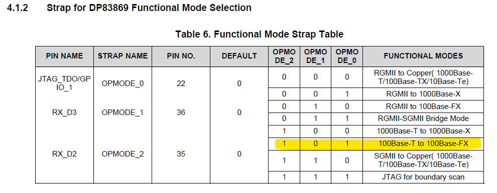
    thank you for the answer. The straps on eval-board DP83869EVM are configured for media converter mode 100BaseT to 100BaseFX according to user's guide Page 12:

    The SerDes-IC we use has a 125MHz refclock and needs an input parallel data signal with an edge offset 2-7ns relative to 125MHz clock. If it has an another offset, error may occur. In this case phase offset between SO_P/N output and clock input must have either permanent value at any power up, or get some value from defined area, but not a random one.

    Best regards,

    Arsenii

  • Hi Arsenii,

    If I understood your application correctly, you need a 125MHz clock output which is synchronous to the 25MHz input clock to the PHY. I will need to review the PHY features and see if there are internal options that will allow such an output. I will get back to you by end of next week. Please correct me if I have misunderstood your requirement.

    -Regards

    Aniruddha

  • Hi Arsenii,

    We do not have a clock that is synchronous to the 625MHz SGMII signal. However, we do have the ability to output the clock used for transmitting data on MDI channels. This is described in register 0x170. The transmit (and receive) clocks for each channel are 125MHz. Is that something that you can use for your application?

    -Regards

    Aniruddha

  • Hi Aniruddha,

    thank you. Unfortunately we do not have an abitily to read or set up the register values, except of strap-resistors.

    Best regards

    Arsenii